Low energy XRF (LE-XRF) in semiconductor metrology with the Sigray AttoMap system Part 1 – Presentation of the system
Micro X-ray fluorescence (µXRF) has proven to be an invaluable analytical technique in the semiconductor industry as it enables non-destructive elemental analysis with high sensitivity for dopants and thin film thicknesses. µXRF is usually performed at high X-ray energies (> 5 keV) and is considered a measurement system for high atomic number (high Z) elements. However, it is often overlooked that µXRF is even more powerful at lower X-ray energies. In this article, we present some application examples of the AttoMap system at low energies for critical applications in semiconductor metrology.
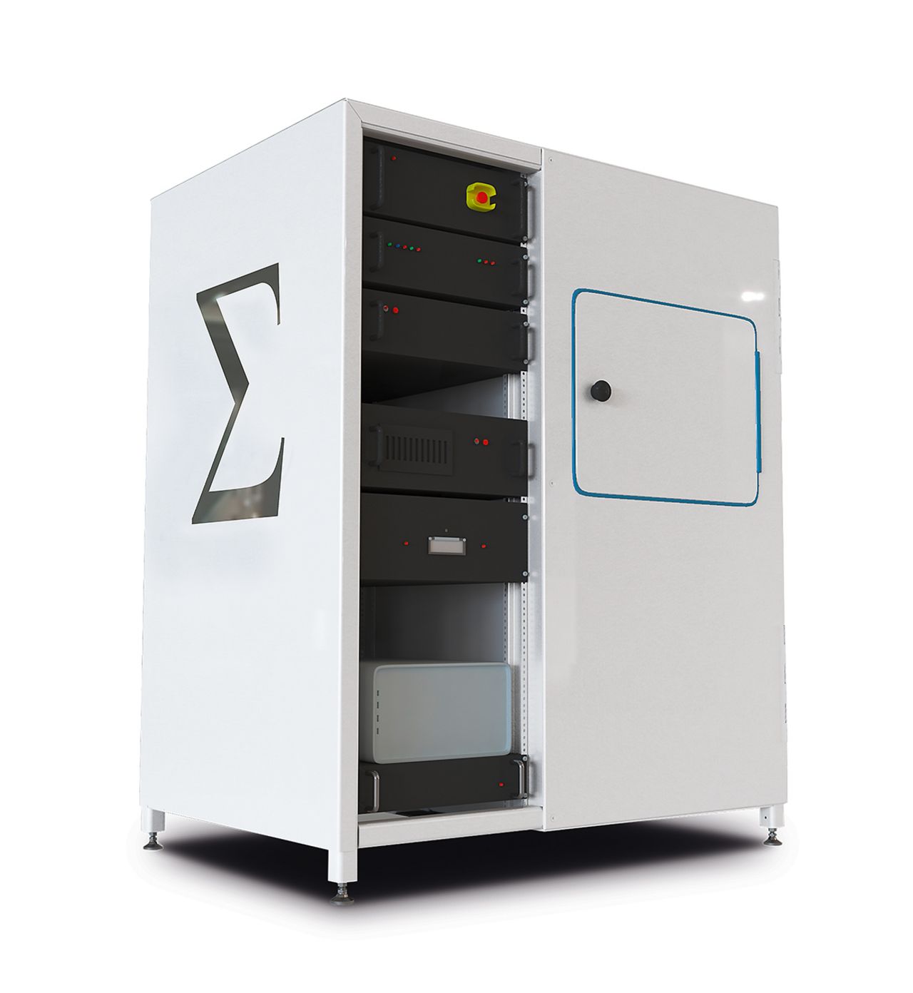
Overview of the AttoMap-310
Performing µXRF at low X-ray energies offers significant advantages over conventional µXRF at higher energies. This includes orders of magnitude higher sensitivity to low-Z elements and even significantly improved sensitivity and shorter acquisition time for the lower energy (L and M lines) of high-Z elements, as the X-ray optics increase with the square of the wavelength. Despite the numerous advantages, the main bottleneck with low energy µXRF is the low brightness of X-ray sources that produce low energy X-rays and the significant challenges in manufacturing X-ray optics for lower energies. The AttoMap-310 utilizes Sigray's patented X-ray source design, which uses actively cooled diamond to achieve high power loading, and its highly efficient axially symmetric X-ray optics. The system has been rapidly adopted by the semiconductor industry [1] for a wide range of elemental analysis applications including:
- Aluminum, for work function adjustment in transistors
- Fluorine, a residue from processing (e.g. etching)
- Germanium used in SiGe structures for gate-all-around applications and as a metrological endpoint for etching
- Molybdenum nitride, which is often used as a thin film in gate electrodes and in memory applications
Other applications include boron, titanium nitride, oxygen and zirconium oxide.
AttoMap-310 micro X-ray fluorescence microscope (µXRF):
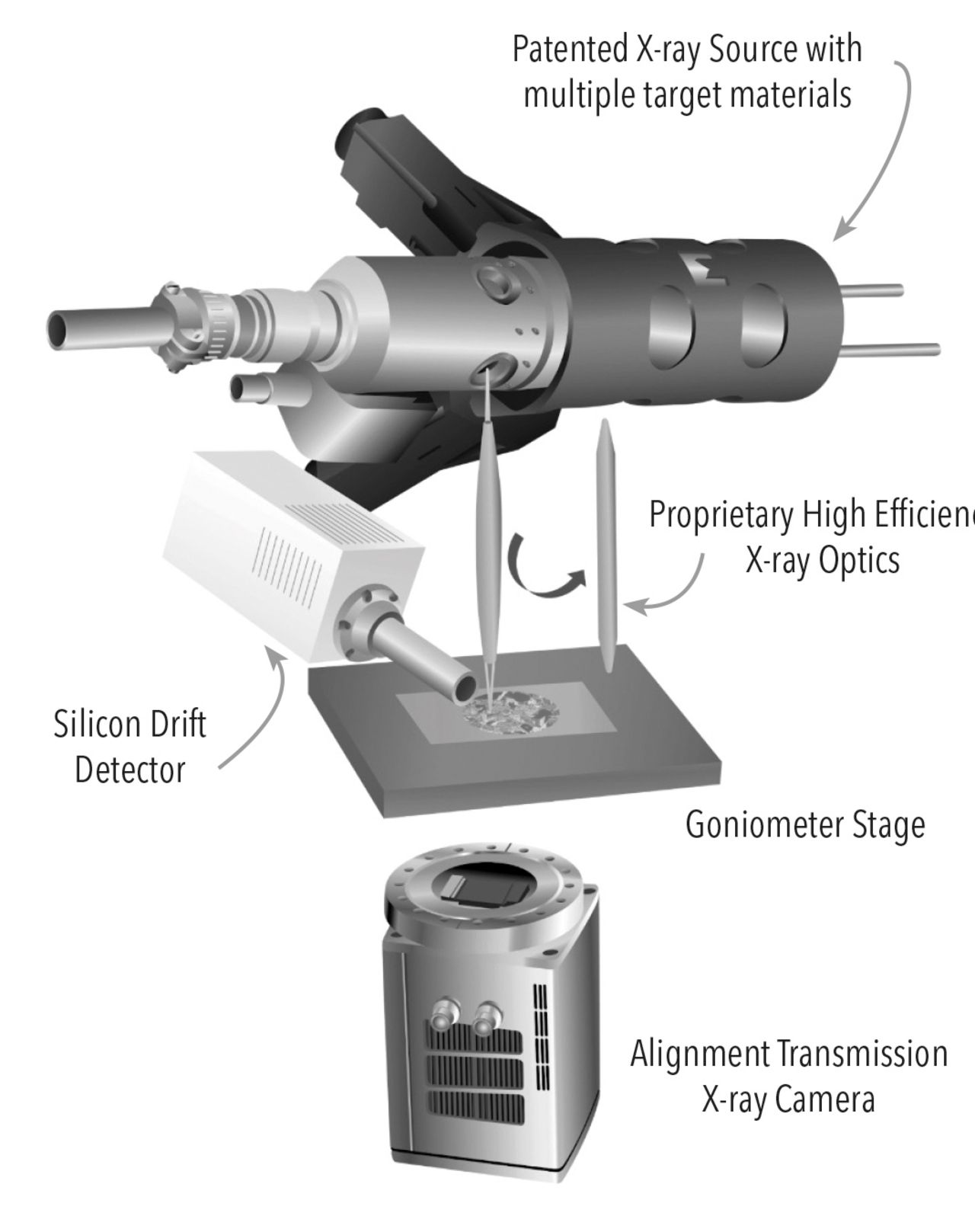
Sigray's AttoMap-310 µXRF enables rapid analysis of both low atomic number elements (low Z) down to boron (B) and low energy fluorescence lines (e.g. L and M lines) of high atomic number elements. Its unprecedented performance is made possible by several key innovations in critical X-ray components, including:
- Patented X-ray source with multiple targets
Sigray's X-ray source allows users to select up to five different X-ray target materials to tune the incident X-ray energy, maximizing sensitivity by up to two to three orders of magnitude. Targets include Sigray's patented ceramic X-ray source targets, which offer significantly higher power loading and higher brightness compared to conventional X-ray target materials such as aluminum. Particularly advantageous targets for semiconductor applications are Sigray's SiC X-ray targets, which produce an ultra-bright Si line that avoids excitation of the Si fluorescence of the substrate/wafer, and a calcium-based target for high-efficiency Sn/Ag ratio measurements. Other targets are Au, Cr, Cu etc. - Proprietary X-ray optics
Unlike conventional µXRF systems that use polycapillary optics, the AttoMap-310 utilizes Sigray's proprietary axially symmetric X-ray optics. This optic provides higher performance at low X-ray energies and can be designed to deliver >99% of an X-ray beam within a 40 µm test field (or focused on a small 3-5 µm achromatic X-ray spot). Sigray optics also allow the detector to be placed much closer to the sample than polycapillary optics, resulting in much greater fluorescence detection. - Goniometer table (θ-2θ)
The sample stage and SDD of the AttoMap-310 can be rotated to achieve near grazing incidence angles on samples to maximize the sensitivity of low energy X-rays. Rotation angles can also be adjusted to remove diffraction peaks in Si wafers. - Vacuum housing
The AttoMap-310 utilizes a vacuum chamber that achieves <10E-5 Torr and is designed to allow ultra-low concentrations of carbon and oxygen at the request of semiconductor customers.
In the next part of our series on low-energy X-ray fluorescence (LE X-ray fluorescence) in semiconductor metrology, we present initial measurement results for aluminum, fluorine, germanium and molybdenum nitride samples.