Visualizing the structural evolution of thermally-decaying platinum nanowires
Metal nanowires represent a main class of one-dimensional nanomaterials and have been proven essential for a wide range of applications. Previous works on electrodeposited nanowires focused on ex situ SEM characterization, which is limited in terms of resolution and unable to monitor internal nanostructure changes. Using the DENSsolutions Wildfire system, Torsten Walbert and his colleagues from the Materials Analysis group and Prof. Leopoldo Molina-Luna from the Advanced Electron Microscopy (AEM) Division at the Institute for Materials Science, TU Darmstadt were able to investigate via in situ TEM the influence of temperature on polycrystalline platinum nanowires. Observing this process under remarkably high resolution enabled them to capture for the first time the internal transformations during both early and intermediate stages of the platinum nanowire decay.
The structural evolution of nanowire decay
Although nanowires are crucial for a wide range of applications, they are frequently prone to degradation. It is important that we understand these underlying failure mechanisms to better ensure reliable performance under operating conditions. Previous studies observing the thermal decay of nanowires have typically focused on ex situ investigations inside an SEM. Only a handful of studies look at the in situ characterization of nanowire decay using TEM, but even those focus specifically on gold nanowires. In this study, Torsten and his team observe the temperature influence on the degradation of platinum nanowires. Platinum is used due to its high mechanical, chemical and thermal stability as well as catalytic activity.
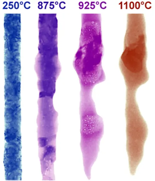
Below you can see an overview of the morphological transformation of a platinum nanowire after a thermal treatment between 250°C and 1100°C. It is observed that the main external transformation starts after 800°C, illustrated by the corresponding diameter evolution.
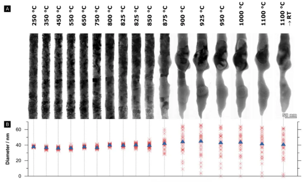
The morphological transformation of a platinum nanowire after thermal treatment and corresponding diameter evolution
Changes in internal nanostructure
Although external shape transformations occur after 800°C, changes in the internal nanostructure happen a lot earlier at markedly lower temperatures. As shown in the figure below, after heating to 250°C, no pronounced changes in the internal structure are observed compared to the initial state. After increasing the temperature to 450°C, the nanowire outline is still unaltered, but voids of low contrast (indicated by red circles) already start appearing. At 800°C, these voids begin to propagate and the shape slightly changes.
Further increasing the temperature to 850°C causes a grain boundary to extend, which is indicated by the dashed green line in the figure below. Finally, at 875°C, the grain boundary straightens while the voids increase and accumulate. Ultimately, these results confirm that internal nanowire restructuring considerably precedes the permanent changes of the outer nanowire shape. In fact, the observed faceted voids and grain boundaries are crucial factors guiding their transformation and final splitting, which is discussed in the next section.
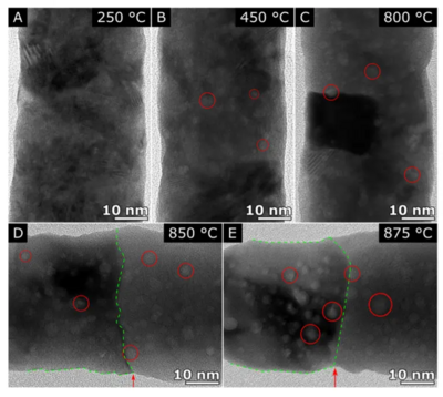
TEM image showing the formation of voids (red circles) and straightening of grain boundary (green dashed line) at low and high temperatures
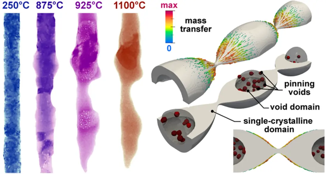
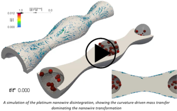
Two surprising domain types
Some surprising results are observed after when the temperature goes beyond 875°C. Interestingly, the nanowires segregated into two domain types, one being single-crystalline and essentially void-free, while the other preserves void-pinned grain boundaries. This is the first time in academia that researchers observe this type of segregation, as it was neither described in previous experimental studies nor predicted by simulations.
You can see in the simulation and TEM video below that the wire separates into two domains, a single-crystalline domain and void-containing domain. Whereas the single-crystalline areas exhibit fast platinum transport, the void-containing areas show an unexpected morphological stability, retaining their nanostructure even at temperatures above 1000°C. In fact, the subsequent splitting of the nanowires is only observed in single-crystalline areas and thus leads to the formation of fragments with varying lengths and diameters.
 |  |
Novelty in findings
Performing in situ TEM in a controlled temperature environment represents a powerful approach for investigating the structural transformations of metal nanowires. Obtaining detailed insights into the internal nanostructure of nanowires and their evolution over time would otherwise be impossible without in situ TEM. Torsten and his team were able to relate the onset of shape changes to distinct nanostructural features acting as starting points in the disintegration process. This study is not only of great interest for basic research, but also helps in predicting the thermal robustness and reliability of nanowires in devices and can serve as a synthetic tool, enabling the control over the disintegration sequence via defect engineering. If we can understand the mechanism behind the process of decomposition, we can better predict and control the thermal stability of nanowires, adapting their shape and properties according to specific applications and conditions.
Original article by Torsten Walbert, Falk Muench, Yangyiwei Yang, Ulrike Kunz, Bai-Xiang Xu, Wolfgang Ensinger, and Leopoldo Molina-Luna
| +39 06 5004204 | |
| +39 06 5010389 | |
| renziqd-europe.com |