FusionScope & Kleindiek micromanipulators: Precise nano characterization
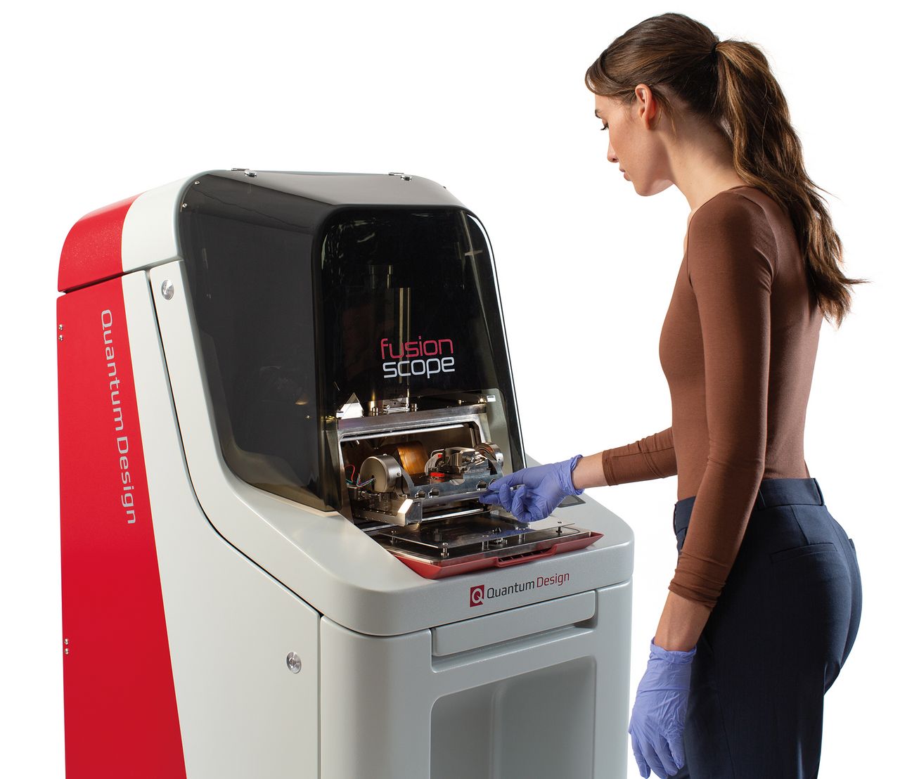
The growing demands on nanoanalysis require innovative methods for high-resolution, in situ, and multimodal characterization. The FusionScope, a combination of atomic force microscopy (AFM), scanning electron microscopy (SEM), and energy dispersive X-ray spectroscopy (EDX), enables comprehensive analysis of nanoscale materials. The integration of high-precision Kleindiek micromanipulators allows samples to be manipulated, electrically contacted, and precisely positioned—an ideal solution for applications such as nanowire characterization, electrical probing, and electrochemical investigations.
Innovative measurement options for nanowires
Nanowires play a key role in modern nanoelectronics. Their mechanical and electrical properties determine their suitability for use in components.
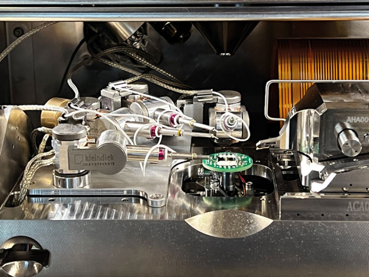
In an experiment, a free-standing ZnO nanowire was precisely placed and positioned under the AFM cantilever. The FusionScope Profile View option (80° tilt function) enabled precise adjustment of both the AFM and the manipulators on the sample surface


The electrical conductivity was determined using IV curves – the wire exhibited ohmic behavior with a resistance of 230 kΩ.
Combined electrical probing & EFM analyses
The parallel use of micromanipulators and AFM enables complex electrical measurements to be performed:
Targeted electrode contacting with two micromanipulators in a multi-electrode probe for simultaneous C-AFM measurement.
Electrostatic investigations (EFM) of an isolated gold area on a silicon sample showed clear contrasts between contacted and non-contacted areas.
Advantages of the FusionScope micromanipulator combination
Multimodal analysis – AFM, SEM & EDX in one platform for comprehensive material characterization
Nanometer precision – Controlled manipulation & exact placement
High efficiency – Fast switching between mechanical, electrical & chemical measurement methods
The FusionScope in combination with Kleindiek micromanipulators offers unique possibilities for high-precision nanoanalysis – from the development of nanoelectronic components to the analysis of complex material properties.
More about the easy-to-use Correlative AFM/SEM Microscopy Platform