LE-XRF in semiconductor measurement technology: Experiments & results with Sigray AttoMap™ – Part 2
Experiments and results
The AttoMap-310 was developed for high-precision µXRF analysis (Al, F, Ge, Mo, N) in semiconductor research. The combination of Sigray's patented SiC anode and axially symmetrical X-ray mirror lenses enables unprecedented signal quality for measurements in the low energy range.
I. Aluminum:
Aluminum is an essential material in modern transistors. To accurately measure Al thicknesses in the sub-angstrom range, a system must efficiently excite Al. Previous LE-XRF methods are limited because Al-based sources do not excite Al, and higher energies (e.g., Cr-Kα, 5.4 keV) generate Al fluorescence but also cause interfering background noise due to Si fluorescence (1.74 keV) and inelastic scattering.
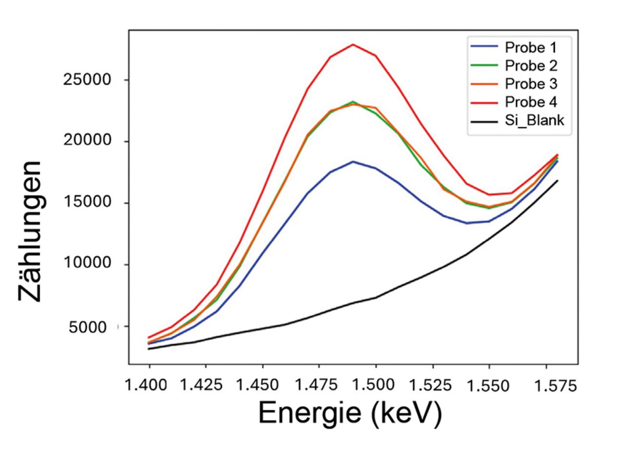
Fig. 1
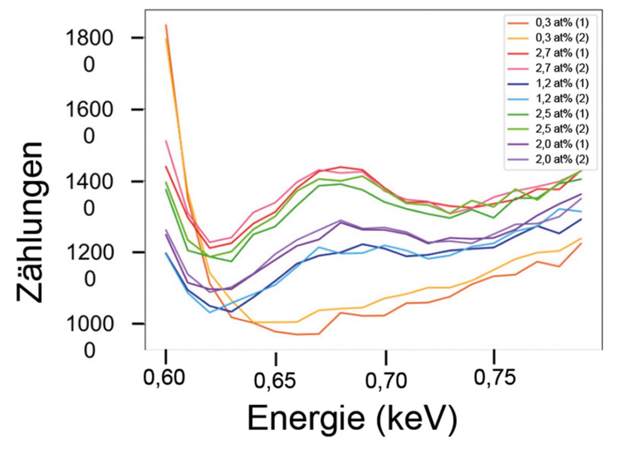
Fig. 2

Fig. 3
sed X-ray target that generates a nearly monochromatic 1.74 keV beam—ideal for Al excitation without stimulating the Si substrate (absorption edge: 1.84 keV). This amplifies Al fluorescence (Kα: 1.56 keV) by >700 times compared to Mo-Kα.
A leading semiconductor manufacturer provided four samples for testing, including a ladder-shaped series of ultra-thin Al layers. Although the exact thicknesses were not specified, the measurements corresponded to the expected spectral trends (Fig. 1).
II. Fluorine:
Fluorine is used in semiconductor manufacturing for etching and cleaning processes, but must not leave any residues as it can cause defects, doping effects, and corrosion. A sample with staggered F concentrations up to 0.3 At% was examined with AttoMap and supplemented with XPS analysis.
Fig. 2 shows the raw spectra of the F peak (0.677 keV). To determine the net counts, a Gaussian fit was performed and the background was subtracted. The linearly correlated net counts (R² = 0.956) demonstrate the high sensitivity of the system to F.
III. Germanium:
Ge is relevant in high-speed electronics, optoelectronics, and for gate-all-around transistors (GAA). In measurement technology, SiGe layers are removed by etching, which is why precise residual analysis of Ge is important.
Conventional high-energy µXRF techniques use Ge-Kα (9.8 keV), but lower energies increase the Ge fluorescence signal due to stronger absorption (Fig. 3). Thanks to the high brightness of the Si source and the larger collection angle optics of AttoMap, a >100-fold improvement in sensitivity and speed is achieved compared to conventional high-energy µXRF methods.
IV. Molybdenum nitride:
Thin MoN films are essential for semiconductor technology, including as gate electrodes and diffusion barriers. Properties such as work function, specific resistance, and thermal stability can be optimized by varying the Mo/N ratio.
Three samples with different Mo/N dosages were scanned with AttoMap. For maximum sensitivity, Mo Lα (2.292 keV) was used instead of Kα (17.4 keV), which enables a >57-fold increase in sensitivity. In addition, N Kα (0.392 keV) was detected.
Summary:
The AttoMap-310 µXRF system sets new standards in semiconductor analysis and enables:
Ultra-high-precision Al measurements down to the sub-Å range
Highly sensitive fluorine residue analysis for quality control
Efficient Ge characterization in SiGe/Si layers
Precise MoN thin film measurements with maximum sensitivity
Thanks to high signal strength, minimal background noise, and innovative X-ray optics, AttoMap offers a superior solution for demanding semiconductor investigations.
Contact
| +49 6157 80710-12 | |
| +49 6157 80710912 | |
| Write e-mail |