In Situ TKD Stage
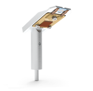
DENSsolutions now introduces an in situ TKD stage for Scanning Electron Microscopes (SEM). For the first time in the market, this stage allows you to perform microstructural characterization using Transmission Kikuchi Diffraction (TKD) while heating or biasing your sample.
The TKD stage will save you valuable time on the TEM, as you can now perform a quick preliminary in situ sample characterization inside the SEM that would have otherwise taken you much longer to accomplish using the TEM.
Applications
In situ characterization of the grain size and distribution, crystal orientation and texture, phase of materials like metals, ceramics, semiconductor and composites from various applications fields such as automotive, aerospace, electronics, power generation, etc.
4 reasons to get the new TKD stage
1. High resolution orientation maps
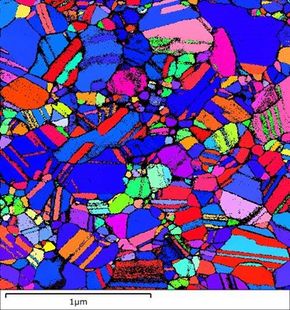
Thanks to its unique geometry, the stage allows you to perform analysis using the Transmission Kikuchi Diffraction method (TKD). Resulting in improved spatial resolution and simplified grain orientation mapping. Enabling quantitative characterization of electron transparent crystalline nanomaterials with ultrafine grains ranging from 10 to 100 nm.

Image courtesy of University of Sydney
2. Easily interchange your chips
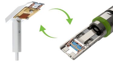
The TKD stage is fully compatible with all double tilt Wildfire and Lightning chips. This means that you can reach the exact same temperatures and voltages inside the SEM as you can with the TEM while easily swapping chips between microscopes.

3. Experience uniform workflow
Both the TKD stage and our In Situ TEM solutions use the same stimuli supply components and control software. This makes it especially convenient for existing customers to add the TKD stage to their workflow.

4. High level of compatibility
The TKD stage is compatible with several Thermo Fisher Scientific (FEI), Zeiss and JEOL SEM/FIB devices and compatible with several Bruker and Oxford instruments detectors*


