In situ MFM analysis of nanostructures with the AFSEM
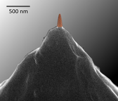
Nanoscale magnetic materials are highly useful for applications in fields like spintronics, thermoelectrics, nanoelectronics and information technologies. Currently, one of the main application fields of these materials is data storage. Focus Electron Beam Induced Deposition (FEBID) is a special technology used to produce nanoscale magnetic materials. It combines very high resolution with direct-write capabilities. Our partner GETec uses this technology to fabricate their so-called “super tips” for MFM imaging. To achieve this, CoFe is deposited on the AFM-cantilever tip with a radius of approx. 10 nm (fig. 1).
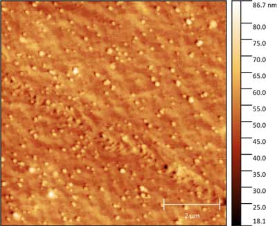
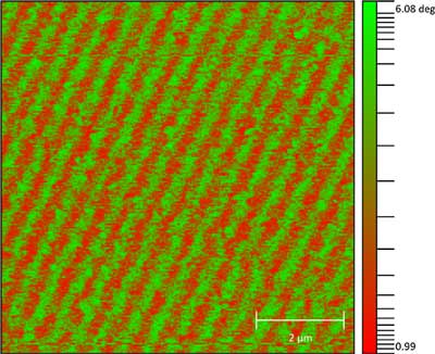
These tips enable analyses of the magnetic properties of a sample at very high resolution in an AFM. However, the magnetic response must be separated from the topographic response. This is done by taking two scans consecutively. First, the AFM cantilever scans the sample in regular AFM mode to obtain the topography (fig. 2). Then, the tip is lifted off the sample and scans the surface at a defined distance. The tip follows the established topography so that the distance between tip and sample remains the same. This way, it only detects the long-range magnetic properties (fig. 3).
For further information, please contact us.


