Metasurfaces and Metalenses
Lenses are widely used as a basic optical element in everyday life. They are used in cameras, eyeglasses, microscopes and many other devices. In this context, the lenses are developed on the basis of classical refractive optics, which leads to unavoidable imaging errors such as chromatic and spherical aberration and coma. To minimise these errors, conventional imaging systems usually use multiple lenses with different powers and different materials.
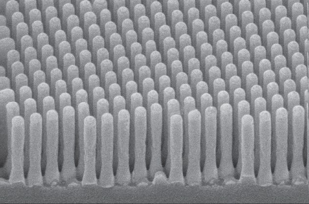
Metasurfaces and metalenses offer high potential as substitutes for many classical optical components. They are a fundamentally new method of light manipulation that is based on scattering in nanostructures instead of conventional refraction, thus allowing efficient phase, polarisation and emission control.
They are able to precisely influence the wavefront of light, thereby producing impressive optical phenomena. Moreover, they are usually significantly smaller and less expensive than conventional solutions. With multidimensional metasurfaces, novel functions can be achieved that are difficult or impossible to achieve with conventional lenses.
Our partner Moxtek has been producing nanostructured optical components for over 20 years, with high-volume manufacturing capabilities for the most different structures on Ø200mm wafers.
The range offered includes the production of functional nanostructures such as microlens arrays, waveguides, patterned metasurfaces, diffractive optical elements (DOE), photonic crystals and biosensor arrays. These components for imaging, illumination and display systems are used for a variety of applications, including automotive, medical and dental imaging, camera systems and many others.
Prototyping samples can be created based on our own in-house developed design master shuttle. This NIL (NanoImprint Lithography) design master shuttle provides space for multiple (different) design structures, allowing multiple designs to be tested in a single shuttle iteration. This dramatically reduces development time and cost. These design shuttles are created several times a year.
We will be happy to discuss your metalens or optical nanostructure needs. Feel free to contact us any time


