MicroWriter – Our Direct-Writing Lithography System with Clever Features
High resolution and fast writing - these are the typical requirements for a direct-writing photolithography system. However, high resolution compromises writing speed and vice versa. For this reason, the developers of our MicroWriter systems have put much thought into the question of how these two requirements can be reconciled as far as possible. Even the first generation of the MicroWriter allowed the user to select different resolutions for different objects. The highest resolution is selected only for those objects for which high resolution is really important, whereas a lower resolution is chosen for objects for which high resolution is not an absolute must, which comes with the benefit of a higher writing speed.
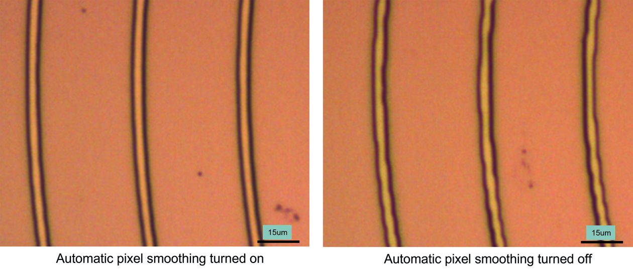
This basic principle is now extended by various options for the writing quality - irrespective of the resolution used. The feature "Automatic Pixel Smoothing" gives users the option to decide about the quality of the edges of the structures to be written. The example in figure 1 shows the difference. The gap width of the coil is 2.5 µm and the resolution of writing was 1 µm. The roughness of the edges can typically be observed in the outstanding range of 30 nm. If this feature is not used, the writing speed increases dramatically, however, at the expense of edge quality.
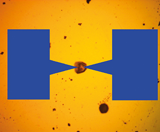
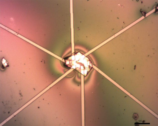
The second important feature is the so-called "Virtual Mask Aligner", which offers the possibility of placing the object to be written over the optical image of the sample surface. This is very help-ful if structures to be written are to be aligned with structures that are already on the surface. A typical example are contact pads for e.g. graphene or 2D materials. Figure 2 shows how this looks in the software, while figure 3 is an actual result from one of our customers (courtesy of UGC-DAE Consortium for Scientific Research, Indore, India).
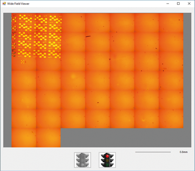
The last feature is the "Wide Field Viewer". This feature allows you to quickly and easily generate a larger overview image of the sample surface. The system automatically circles the starting point, capturing one optical image at a time. Each further image will be stitched together to create an ever larger overview image. This feature can be used, e.g., to find alignment markers or to look at already written structures for a first inspection.


