New medium for quantum networks
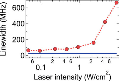
An important prerequisite for creating a quantum network is a scalable system consisting of quantum bits (qubits), in which quantum information can be processed. Semiconductor systems are the obvious choice for this purpose, since the manufacturing processes are already known from semiconductor electronics. Alternatives such as nitrogen vacancies (NV centers) in diamonds have excellent optical properties [1], but are much more difficult to produce on an industrial scale. However, common semiconductor systems have two major disadvantages: Strong interaction of the electrons with lattice vibration (phonons) and thus a correspondingly low intensity of the interference-free zero phonon line (ZPL). Moreover, the times for spin dephasing are short, so that information can only be stored for a short time. Roland Nagy of Jörg Wrachtrup’s team at Stuttgart University has now discovered a new semiconductor system that does not have these disadvantages anymore [2]. The extremely long coherence times make these qubits an excellent choice for memory-assisted quantum network applications based on semiconductors. Moreover, the optical resonances are very sharp. The absorption line width is close to the limit for Fourier transformations. This allows individual spin states to be targeted optically.
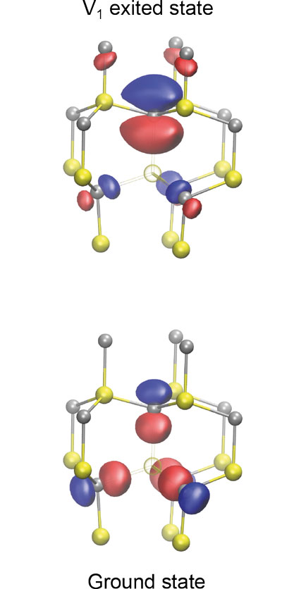
Silicon vacancies (SiV centers) in silicon carbide exhibit very stable optical transitions with little interference from phonons. Coherence times are in the millisecond range and are thus by orders of magnitude longer than those in NV centers, which are in the nanosecond range.
Only at low temperatures the SiV centers are stable enough to allow meaningful experimentation with them. This is something they have in common with other optical defects such as NV centers. At room temperature, the optical transitions are subjected to strong interference due to interaction with lattice vibration. Since the intensity of optical defects is generally low, an objective lens with a high numerical aperture (NA) is required. This proves difficult in cryostats, since the lens must be installed either outside the sample chamber - with a correspondingly high working distance - or as a special cryo version inside the chamber. Both variants have only a moderately high NA. With the Cryostation CO, it is possible, for the first time, to install a heated lens inside the sample chamber. Thus, a high NA (up to 0.9) is achieved, as known from high-end room temperature objective lenses. And, what’s more: One is not restricted to the very limited range of cryo lenses. The lens suspension is actively temperature-stabilized and therefore hardly drifts. This allows long integration times without the need to adjust the sample position.
To align the spin of the defect, a weak magnetic field is required. For this purpose, Wrachtrup’s team has used two permanent magnets outside the sample chamber. Thus, a sufficiently high field is achieved at the sample despite the fact that the sample chamber of the Cryostation is quite narrow.
[1] Humphreys, P. C. et al. Deterministic delivery of remote entanglement on a quantum network. Nature 558, 268–273 (2018).
[2] Nagy, R. et. al. High-fidelity spin and optical control of single silicon-vacancy centres in silicon carbide. Nat. Commun. 10, 1954 (2019)


