Deep-reactive ion etching of silicon nanowires – a groundbreaking method to fabricate nanostructures
The fabrication of nanostructures has made great progress in the last years, particularly in the semiconductor industry and nanotechnology. The recent publication of a consortium of European metrology institutes presents a groundbreaking method to fabricate nanostructures that has the potential to revolutionize the development of nanoelectronics and nanosensors.
The paper, which was published in the Journal of Applied Physics, describes an innovative approach for the fabrication of silicon nanowires by deep- reactive ion etching (DRIE). The technique allows the specific structuring of silicon substrates and the accurate manufacturing of nanowires. By precise control of the ion etching, nanowires with tunable height, width and form can be fabricated, which allows a variety of applications in nanoelectronics, sensor technology and photonics.
One important aspect of this method is the scalability and reproducibility. By using DRIE, nanowires can be manufactured in large quantities, which makes them ideal for the mass production of nanostructures. Furthermore, the precise control of the process parameters allows high reproducibility of the fabricated nanostructures, which is crucial for the development of reliable nanoelectrical devices.

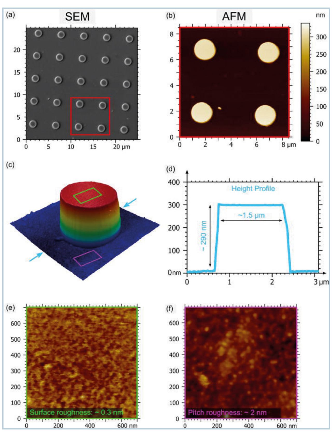
Our sophisticated correlative microscope FusionScope was used to examine silicon nanowires with scanning electron microscopy and measure the surface roughness with atomic force microscopy at the same time.
This technology allows a great variety of applications. Silicon nanowires are used in the semiconductor industry for the manufacturing of nanotransistors, nanosensors and nanoscale components. They can also be used in biotechnology for the development of high-throughput biosensors and in photonics in the manufacturing of nanolasers.
All in all, the publication “Deep Reactive Ion Etching of Silicon Nanowire” is a valuable contribution to the manufacturing of nanostructures. It opens up new ways to fabricate nanoelectronics and nanosensors. With its precise control and scalability, this method has the potential to shift the boundaries of nanotechnology and facilitate new applications in various fields.
Jiushuai Xu et al.; Appl. Phys. Rev. 11 (2): 021411 https://doi.org/10.1063/5.0166284