SWIR imaging of guided and scattered light from silicon PICs

Photonic Integrated Circuits (PICs) are a key enabling technology in application areas from telecommunications and biosensing, to quantum optics. To characterize these planar, optical circuits, it is necessary to couple their signals to laboratory-based measurement equipment by using standard optical fibers.
Given the small waveguide cross-sectional area, it is often difficult to align both input and output fibers to the PIC using only a top, visible microscope image as a positional guide. In this case the power coupled from the output fiber is used to guide the alignment of both input and output.
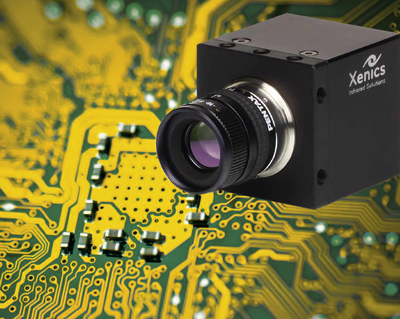
Given the 3-axis translation stage control on both fibers this can be a prolonged task. The alignment can be significantly accelerated by using an SWIR camera. A Xenics XS-1.7-320 InGaAs camera was used for the experiments. The output facet of the PIC chip was imaged onto the camera by coupling the light through an objective lens. Since the full facet is imaged the alignment of the input fibre to the waveguide can be quickly assessed. If the fibre is above the level of the chip then clear interference fringes are visible, while a denser scattering pattern is observed if the fibre is injecting into the substrate.


