
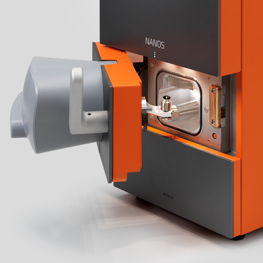

Desktop Scanning Electron Microscope for Imaging and Elemental Analysis – NANOS
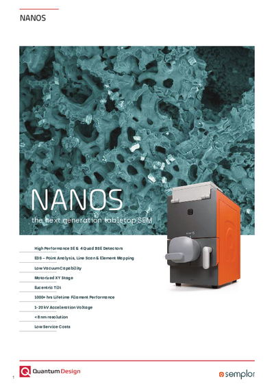
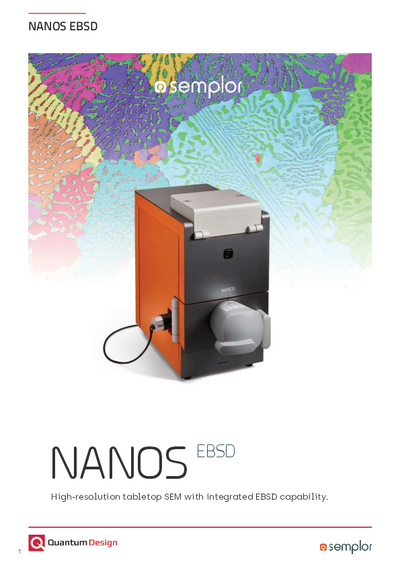
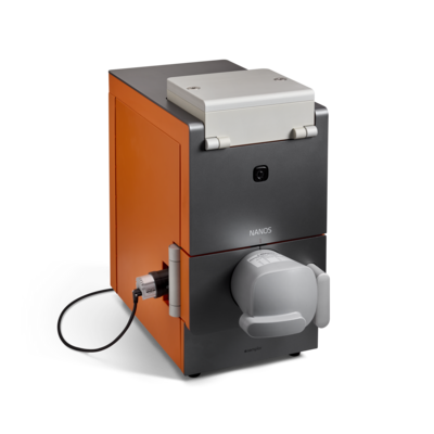
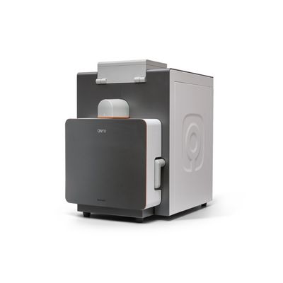
NANOS by SemplorThe NANOS by Semplor is a compact desktop scanning electron microscope for high-resolution imaging, material contrast and optionally integrated EDS analysis. Secondary and backscattered electron detectors provide detailed information on surface topography and material composition. The system combines a compact footprint with flexible sample handling, high- and low-vacuum operation and a motorized XY sample stage.
- SEM resolution < 8 nm and magnification from 100x to 200,000x
- Everhart-Thornley secondary electron detector and four-quadrant BSE detector for topography and material contrast
- Available with or without EDS; fully integrated 30 mm² silicon drift detector in the EDS configuration
- High vacuum and low vacuum at 40 Pa for conductive and non-conductive samples
- Motorized XY sample stage and eucentric tilt from +15° to -40°
- User-replaceable tungsten filament
Further information
Surface Topography and Material Contrast
The Everhart-Thornley secondary electron detector reveals fine surface structures with high detail. The four-quadrant backscattered electron detector visualizes differences in average atomic number and provides material contrast. Its individually addressable segments also enable directional topographic imaging. SE and BSE signals can be overlaid or displayed side by side, allowing direct comparison of topography and composition.

BSE image: differences in material composition
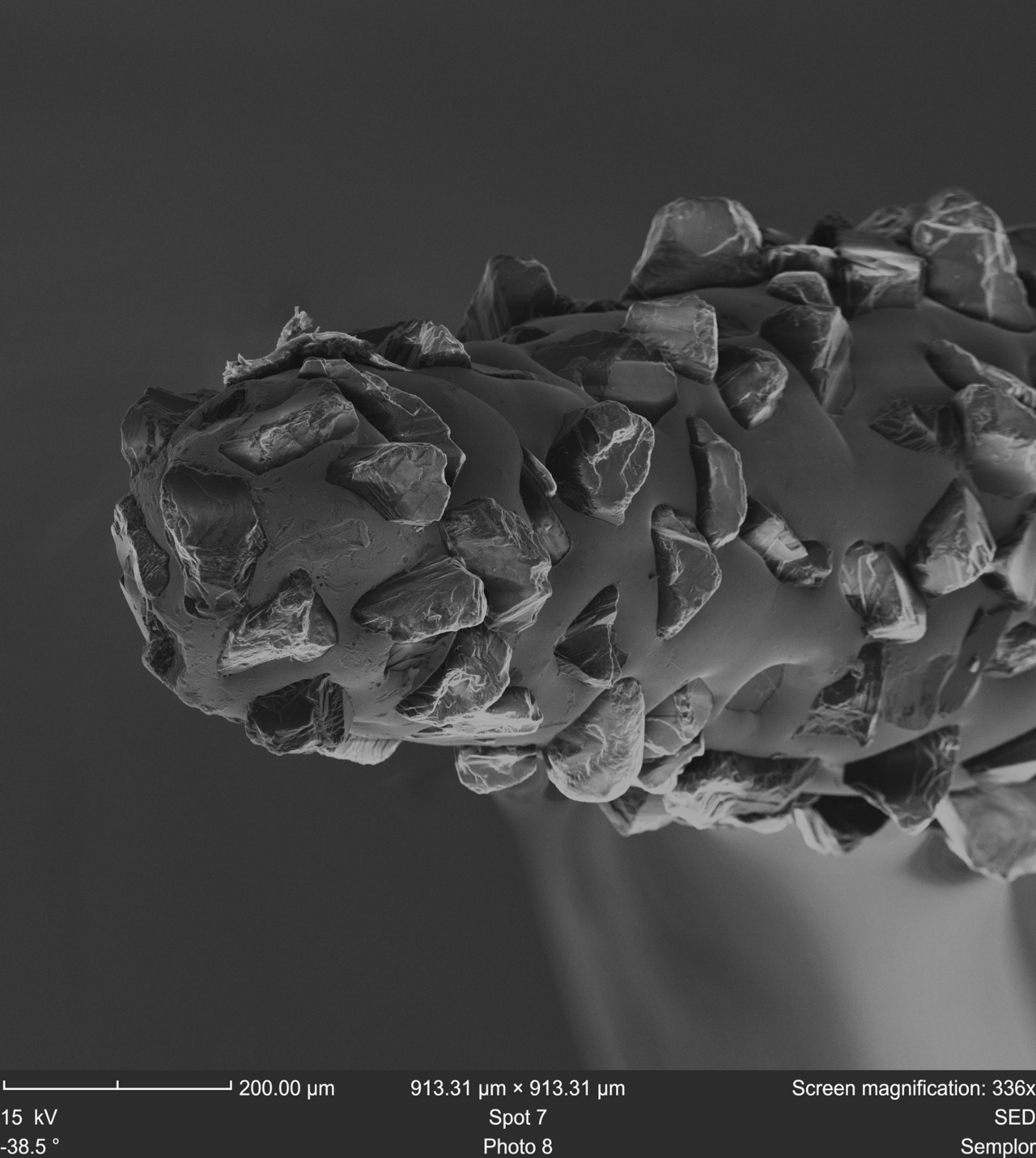
SE image: surface topography
EDS Analysis with an Integrated Silicon Drift Detector
The NANOS can be configured with or without EDS. In the EDS configuration, a thermoelectrically cooled silicon drift detector is fully integrated into the system. The active area is 30 mm², with an energy resolution of < 132 eV at Mn Kα. Elements from boron to americium can be investigated using point analysis, line analysis and spatially resolved elemental mapping.
Discover EDS is available as an optional software module for data evaluation. It combines SEM imaging and EDS analysis in a single interface. Live spectra and live mapping provide visual feedback during acquisition. Automatic peak identification, background correction, peak deconvolution and standardless quantification support data analysis. Measurement data, acquisition parameters and sample positions remain stored within the project for subsequent analysis and documentation.
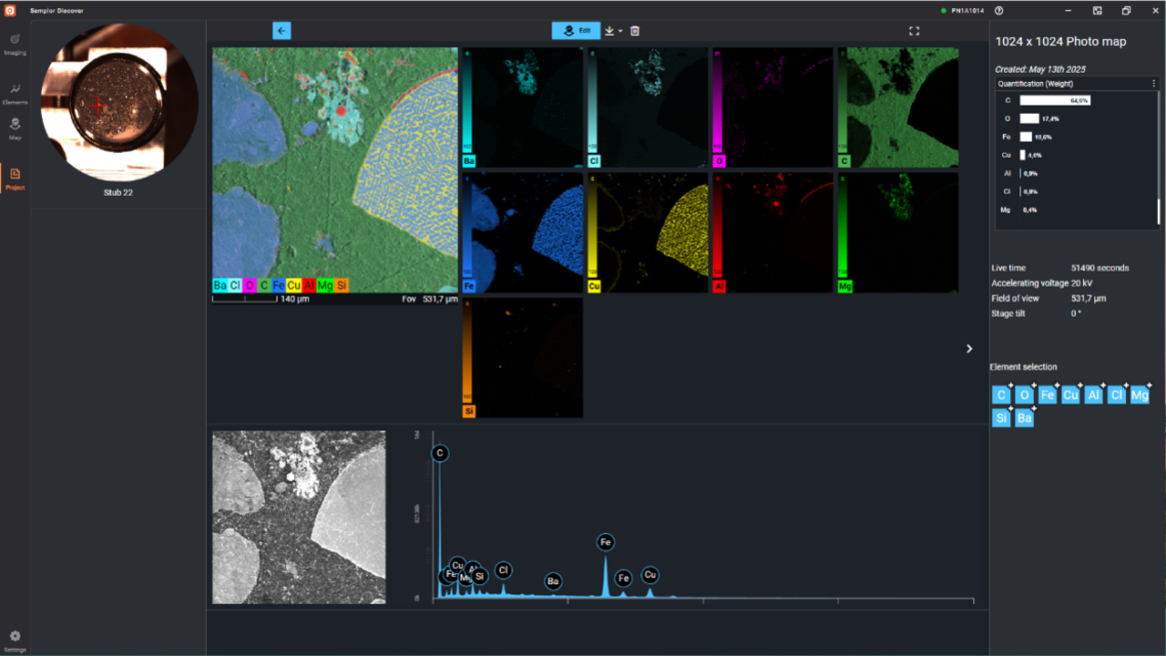
Discover EDS combines SEM imaging, spectrum and spatially resolved elemental maps.
Sample Navigation, Sample Stage and Vacuum
An adaptive color camera captures an optical overview of the sample surface after loading. Regions of interest can therefore be located quickly and approached directly.
The motorized XY stage provides a travel range of 25 x 25 mm. Eucentric tilting keeps the selected sample region in focus while the sample is tilted, and the tilt angle is displayed in the user interface.
The NANOS operates in high vacuum for high-resolution imaging and in low vacuum at 40 Pa. Low-vacuum operation reduces charging effects on non-conductive samples and can reduce sample preparation requirements. Samples up to 45 mm in diameter and 19 mm in height can be accommodated; sample heights of up to 40 mm are available as an option. The available tilt range is reduced when using the maximum sample diameter.
Eucentric tilting keeps the selected sample region in focus.
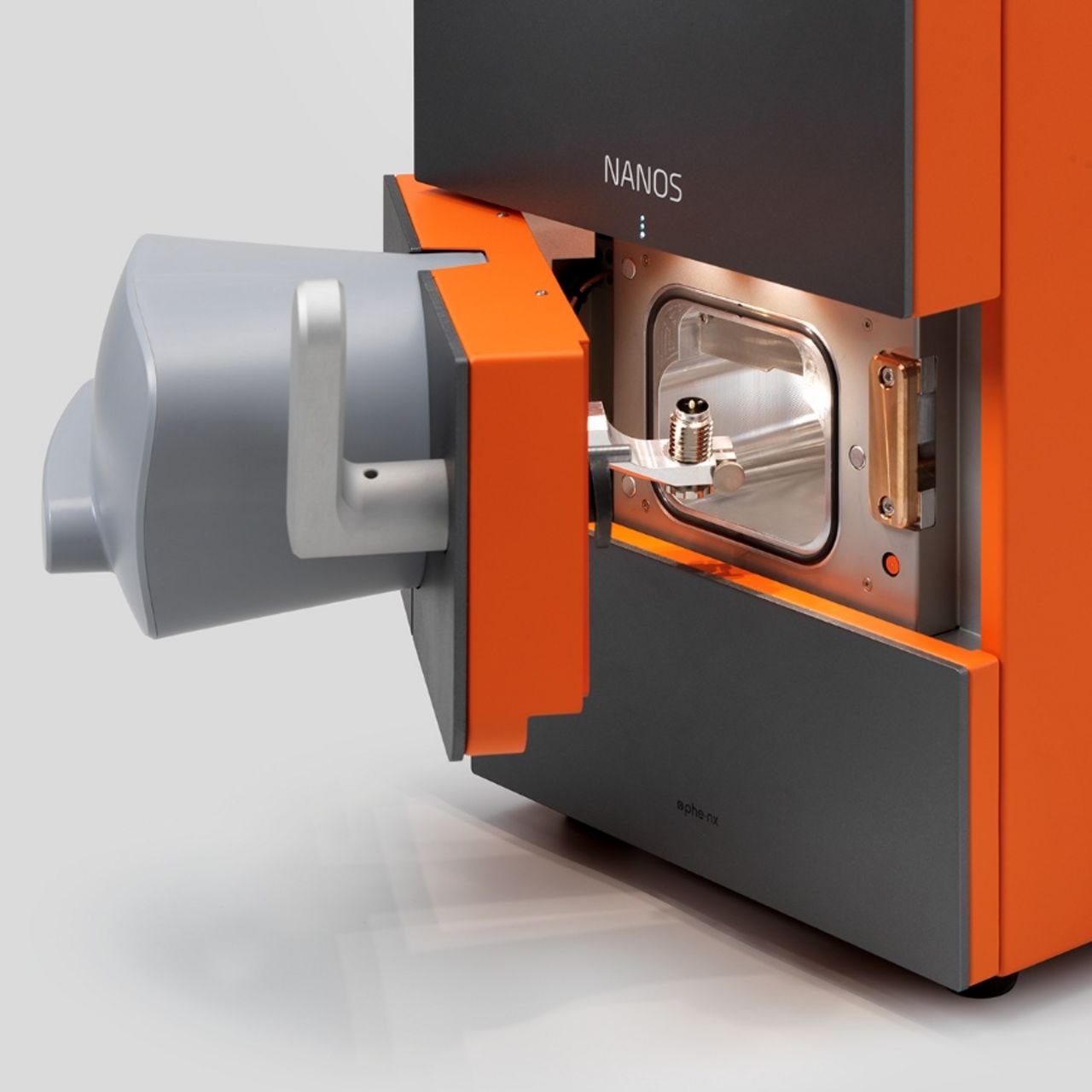
Easily accessible NANOS sample chamber.
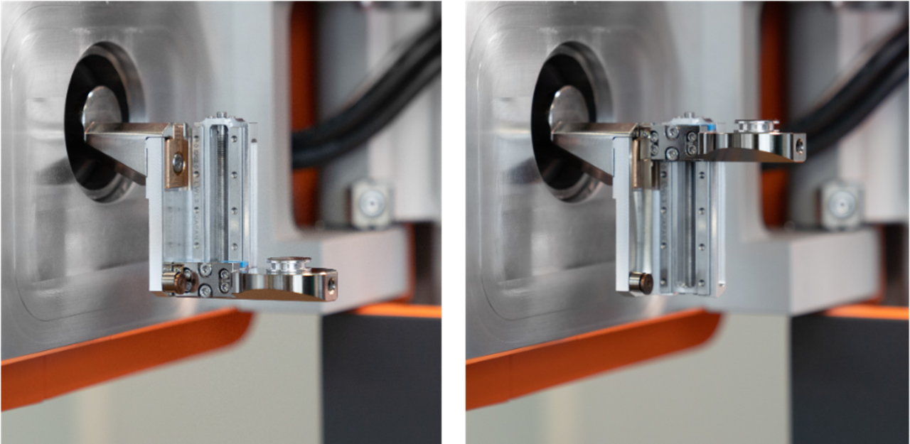
Optional sample holder for samples up to 40 mm in height.
Optional Software Modules for Particle, Fiber and 3D Analysis
The Explore modules integrated into the user interface extend SEM imaging with quantitative analysis capabilities:
- Explore Particles detects, segments and measures particles, pores and grains and provides size distributions and shape parameters.
- Explore Fibers determines fiber length, diameter, orientation and curvature and supports batch processing of larger datasets.
- Explore 3D generates 3D reconstructions, height maps and surface roughness statistics from SEM images.
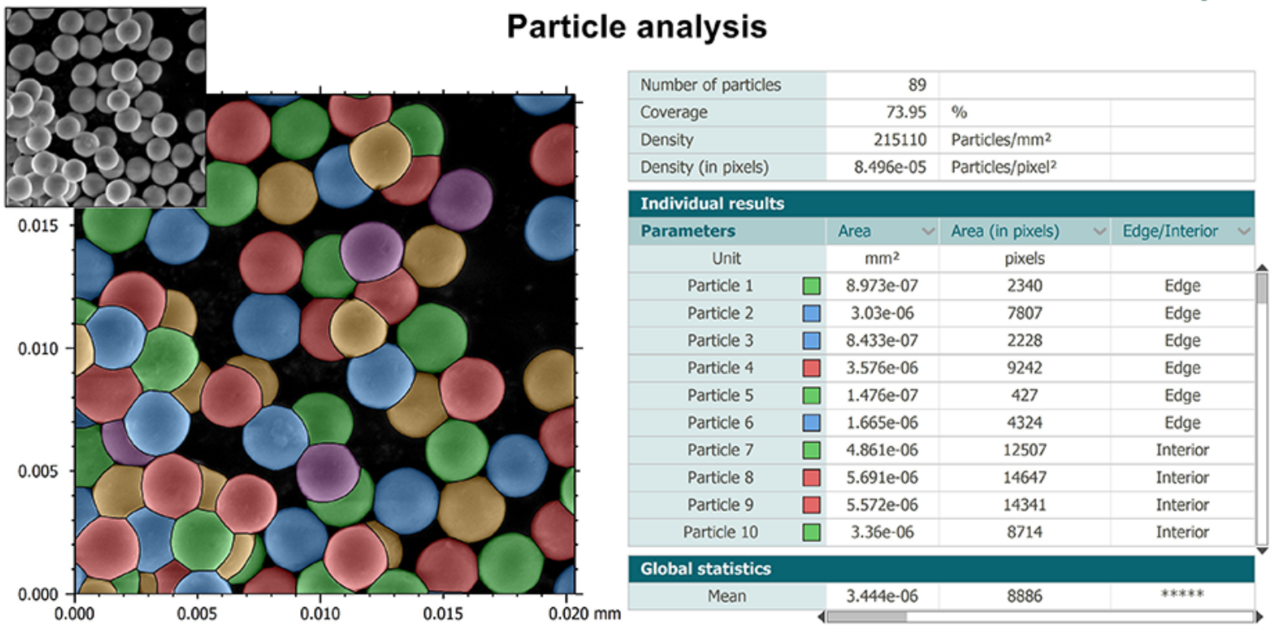
Explore Particles
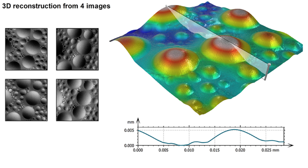
Explore 3D
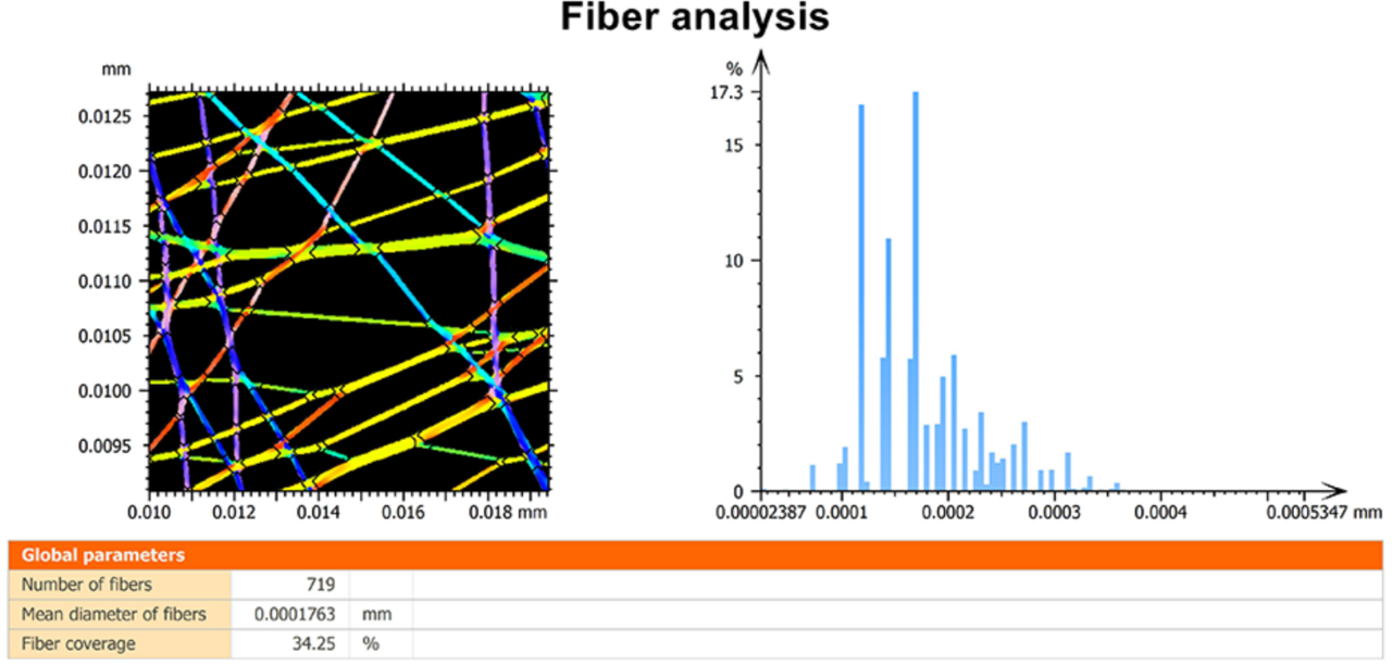
Explore Fibers
Designed for High Availability and Low Operating Costs
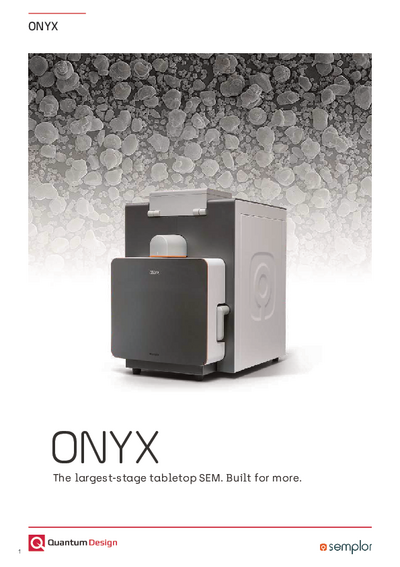
The NANOS does not require a cleanroom or specialized laboratory infrastructure. With dimensions of 280 x 470 x 550 mm and a weight of 62 kg, the system can also be installed in laboratories where space is limited.
The tungsten filament is designed to be replaced by the user, allowing routine maintenance to be carried out without extensive intervention in the system.
Replacing the tungsten filament on the NANOS.
Applications
The NANOS supports imaging, analytical and quantitative tasks in research, development and quality control.
Materials and microstructure analysis: Microstructures, phases, pores, inclusions, fracture surfaces and local elemental distributions in metals, ceramics, minerals and composite materials.
Surfaces, coatings and interfaces: Topography, coating morphology, corrosion, wear, interfaces and defects on functional and technical surfaces.
Particle, pore and powder analysis: Morphology, size, shape and distribution of particles, pores and grains; quantitative analysis with Explore Particles.
Fiber and environmental analysis: Characterization of fibers, microplastics, fine particles and contaminants; quantitative fiber analysis with Explore Fibers.
Failure analysis and quality control: Fractures, foreign particles, residues, technical cleanliness and production-related deviations.
Biological, medical and pharmaceutical samples: Biological structures, biomaterials, implant surfaces as well as active ingredients, excipients and foreign materials, depending on sample preparation and vacuum compatibility.
Specifications
Electron Optics and Imaging
| SEM Resolution | < 8 nm |
|---|---|
| Magnification | 100x to 200,000x |
| Image Resolution | up to 4096 x 4096 pixels |
| Accelerating Voltages | 1, 2, 5, 7, 10, 15 and 20 kV |
| Electron Source | thermionic tungsten source |
| Detectors | Everhart-Thornley SED; four-quadrant BSE detector; Energy Dispersive X-Ray Spectroscopy (EDS) |
EDS – Depending on Configuration
| Detector | thermoelectrically cooled silicon drift detector |
|---|---|
| Active Area | 30 mm² |
| Energy Resolution | < 132 eV at Mn Kα |
| Maximum Count Rate | 300,000 cps |
| Detectable Elements | boron (B, 5) to americium (Am, 95) |
| Analysis Modes | point analysis, line analysis and elemental mapping |
| Mapping Resolution | up to 2048 x 2048 pixels |
Vacuum and Sample Stage
| Vacuum | high vacuum < 1 x 10⁻¹ Pa; low vacuum at 40 Pa |
|---|---|
| XY Travel | motorized, 25 x 25 mm |
| Tilt | manual, eucentric; +15° to -40° |
| Sample Diameter | up to 45 mm |
| Sample Height | up to 19 mm; optional up to 40 mm |
System Data
| Dimensions | 280 (W) x 470 (D) x 550 (H) mm |
|---|---|
| Weight | 62 kg |
| Environmental Conditions | 15-25 °C; 20-80% relative humidity |
| Power Consumption | typically 110 W; maximum 140 W |
Downloads
Contact

Navigation
Categories
Contact
Quantum Design SA
Rue du Nord3
CH-1400 Yverdon-les-Bains
Switzerland
| Phone: | +41 21 8699-033 |
| E-Mail: | suisse@qd-europe.com |
Support