Fast and compact spectroscopic ellipsometer for in situ measurements at ALD layer growth
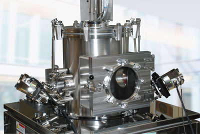
Fig. 1 PicosunTM R-200 Advanced ALD plant with mounted iSE, light source mounted on the left, receiving unit mounted on the right
With iSE from Woollam Co. we offer a compact and fast spectroscopic in situ ellipsometer that has specially been developed for the real-time monitoring of thin film growth. Special “Dual Rotation” design allows the high-resolution measurement of even very small changes of optical constants and film thicknesses with time resolution of 0.3 seconds. This makes iSE the perfect tool for ALD processes. A spectral range of 400-1000 nm enables the measurement of both dielectric and metallic layers and the determination of their thickness during the coating process.
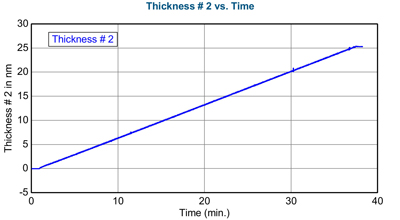
Fig. 2 Al2O3 on silicon. Measured film thickness as function of time. Chuck temperature 150 °C, 300 cycles, cycle-time 7.2 s,
GR= 0.08 nm/cyc, final thickness 25.3 nm
Figures 2 and 3 show measurements of Al2O3- (Fig. 2) and TiO2 layers (Fig. 3) on silicon during the ALD growth process with a Picosun R-200 Advanced ALD system (Fig. 1). You can see the high film thickness and time resolutions that allow resolving even small changes in thickness during the individual ALD growth cycles.
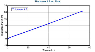
Fig. 3a TiO2 on silicon. Measured film thickness as function of time. Chuck temperature 150 °C, 400 cycles, cycle-time 10.6 s,
GR= 0.054 nm/cyc, final thickness 20.7 nm
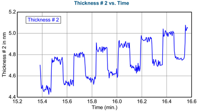
Fig. 3b TiO2 on silicon. Measured film thickness as function of time. Chuck temperature 150 °C, 400 cycles, cycle-time 10.6 s,
GR= 0.054 nm/cyc, final thickness 20.7 nm
The iSE features a broad spectral range. This allows the analysis of metallic layers and the determination of their optical constants and film thicknesses. The film growth of Pt was analyzed with an ALD system FlexAL from Oxford Instruments (Fig. 4).
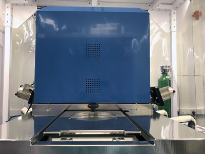
Fig. 4 Oxford Inst. ALD system FlexAL with mounted iSE
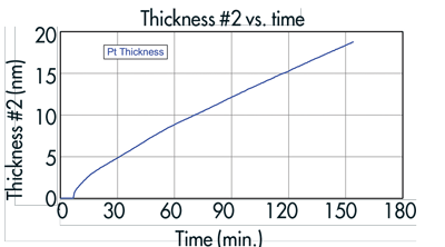
Fig. 5 Pt on Si/SiO2. Measured film thickness as function of time. Chuck temperature 175 °C, final thickness 18.2 nm
Typically, metals do not form uniform layers at the beginning of the growths, but grow in islands. To increase sensitivity in respect of layer thickness and optical constants and to ensure that these parameters don’t correlate during fitting, the so-called Interference-Enhancement-Method was used. First, the Pt film is deposited on a 500 nm thick SiO2 layer (on Si). The film thickness interferences of the dielectric layer are damped with increasing Pt thickness, which provides sufficient sensitivity for all parameters that need to be determined. However, an ellipsometer is needed with a broad spectral range like the iSE.
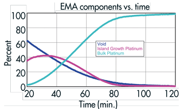
Fig. 6 Change in the bulk, island Pt and void ratio as function of the growth period
Fig. 5 shows the Pt thickness as function of time. Maximum film thickness was 18.2 nm. The Pt layer was modeled with an EMA model using optical constants of bulk Pt, of island-grown Pt and void (air). The proportions of bulk, island-Pt and void were fitted. The change in ratio is shown in Fig. 6.


