FLX Flexus thin film stress measurement systems
From Toho TechnologyToho FLX thin film stress measurement systems allow the determination of stresses and the linear expansion coefficient of thin and thick films on silicon wafers and other substrate materials. The system’s functions are industry standard for mass production and research facilities that demand accurate stress measurements on various films and substrates. Working with KLA-Tencor’s patented “Dual Wavelength” technology, systems of the FLX series accurately determine and analyze surface stresses caused by deposited thin films.
- Available temperature range from -65 °C up to 500 °C
- Patented dual wavelength technology for optimal signal readout
- Calculation of coefficient of thermal expansion and biaxial modulus
- 3D mapping of sample deflection/stress distribution
- Sample sizes from 25 mm up to 300 mm possible
Further information
Theory of operation
Stress is induced when materials dissimilar coefficients of thermal expansion are bonded together. Films may behave similarly at high temperatures, however, as they are cooled, materials may contract or expand differently, causing stress in the film. With a stressed film, defects such as dislocation, voids, and cracking may occur.
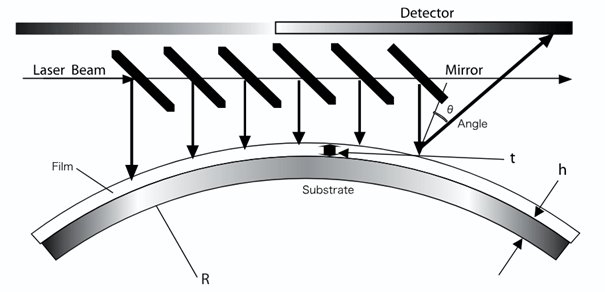
The FLX determines stress by measuring the substrate curvature change of pre and post thin film deposition. The difference in curvature is used to calculate stress by way of Stoney’s equation. The equation relates the biaxial modulus of substrate ![]() , film thickness t, substrate thickness h and the curvature radius R, pre and post process. Curvature is measured by directing two lasers at a surface with a known spatial angle. The reflected beam strikes a position sensitive photodiode. The geometry of the film is then recorded by scanning the surface at selected points.
, film thickness t, substrate thickness h and the curvature radius R, pre and post process. Curvature is measured by directing two lasers at a surface with a known spatial angle. The reflected beam strikes a position sensitive photodiode. The geometry of the film is then recorded by scanning the surface at selected points.
Stoney equation: ![]()
![]() : Two-axis elastic modulus of the substrate (Pa); (100) Silicon gives us 1.805E11 Pa
: Two-axis elastic modulus of the substrate (Pa); (100) Silicon gives us 1.805E11 Pa
h: Substrate thickness (m)
t: Film thickness (m)
R: Substrate radius of curvature (m); 1/R= 1/R2 – 1/R1 (R1: Leading radius of curvature; R2: Trailing radius of curvature)
S: Average film stress value (Pa)
System details
The Flexus-S thin film measurement systems from Toho Technology allow stress measurements in the temperature range -65 °C up to 500 °C. Film stress that occurs during coating processes leads to voids and cracking and thus constitutes one of the main causes for the failure of electronic parts. With KLA-Tencor's patented "Dual Wavelength" technology a laser beam is moved above the sample along an axis. The reflected beam strikes a position-sensitive photo diode. The curvature radius of the wafer along the axis is measured by a line scan before and after the film deposition and hence allows the determination of the change of curvature due to the deposition. The wafer’s film stress is then calculated by way of Stoney’s equation. Several scans along different axes allow the creation of a 3D image of the stress distribution or curvature of the wafer.
The new FLX-R systems are a cost-effective alternative for applications where temperature measurements are not important. Along with the standard FLX functions, they feature an automated rotation stage which rotates the sample around any customer-determined angle and performs several scans. 3D mapping software plots both the three-dimensional distribution of the film stress and the sample deflection.
Flexus stress measurement systems are available in various versions. First, the systems can be categorized according to maximum wafer size: up to 200 mm for the FLX-2320-S, FLX-2320-R, and FLX-2000-A models, and up to 300 mm for the FLX-3300-T and FLX-3300-R models. In this classification, the -S and -T variants feature a temperature platform for variable temperature control, while the -R systems offer automated sample rotation at room temperature. The -A designation denotes a system without temperature control that utilizes manual sample rotation.
Additionally, there is the FLX-2320-L. This is an automated version based on the FLX-2320-R, designed for high throughput through the use of robotic wafer handling from cassette to cassette. It is available in one of two configurations, capable of accommodating either 150 mm and 200 mm wafers, or 100 mm, 125 mm, and 150 mm wafers. The cassette port is designed as a single port in accordance with the SEMI E1.7 standard and is configured to accommodate a 25-slot cassette system. Wafer handling is performed by a single-arm robot utilizing a ceramic, Teflon-coated backside vacuum gripper. A backside vacuum mechanism—constructed from PPS (polyphenylene sulfide)—is also employed for wafer alignment. The wafer rests on a three-point support structure made of PEEK (polyether ether ketone). To ensure a clean process environment, HEPA filtration is integrated into the system's ceiling as a standard feature. Optionally, we can offer an uninterruptible power supply (UPS), a signal tower (3-color, with audible alarm), an integrated earthquake protection system, a barcode scanner (manual reader for open cassettes), an ionizer/ESD control system, a wafer scale, and a ULPA filter.
Specifications
Maximum Scan Diameter/Sample Size
- 50-200 mm for the FLX-2320 (1 inch on request)
- 200-300 mm for the FLX-3300
Performance
- Measurement Range: 1 to 4000 MPa1 (3500 MPa for the FLX 3300)
- Repeatability: 1.3 MPa
- Accuracy: Less than 2.5% or 1 MPa whichever is larger
- Minimum Radius: 2 m
- Maximum Radius: 33 km
Operating Temperatures (for FLX-2320-S and FLX-3300-T)
- Operating Temperature: -65°C to 500°C
- Purge Gas: Nitrogen or Argon
- Gas Flow: 1,5L/min, 0.3 kg/cm²
- Cooling Option: with Liquid nitrogen
- Temperature ramp rate to 500°C: 25°C/minute
- Cooling rate: 500°C to 100°C in 1 hour, 30 minutes with LN²
- Determination of Coefficient of thermal Expansion/biaxial film modulus
Applications
With a stressed film, defects such as dislocations, voids, and cracking may occur. The FLX stress measurement system helps troubleshoot applications listed below:
- Aluminum stress-induced voids
- Passivation cracking (nitride, oxide)
- Stress-induced dislocations in silicon
- Electrical test yield degradation
- Tungsten silicide cracking
- Stress increase in oxides during temperature cycling
- Constant current stress test (CCST) degradation
- Matching metallization expansion on GaAs
- Silicon cracking due to high film stress
- Above issues on thick films (see application note below)
Downloads


Contact

Navigation
Categories
Contact
Quantum Design GmbH
Meerstraat 177
B-1852 Grimbergen
Belgium
| Mobil: | +32 495 797175 |
| E-mail: | beneluxqd-europe.com |