AFSEM nano
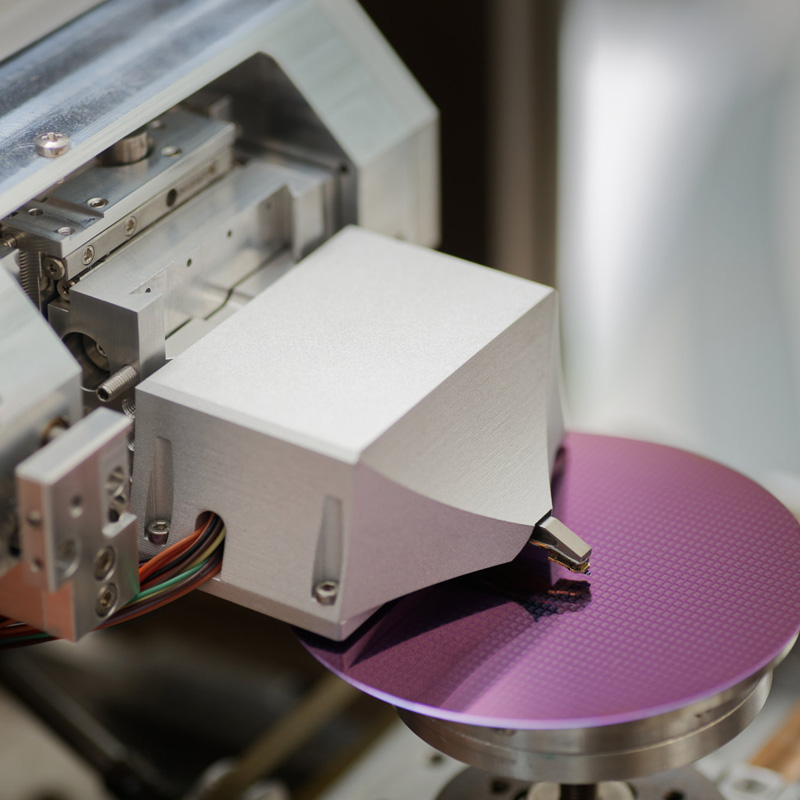
QD-MicroscopyL’AFSEM-nano™ est un microscope à force atomique (AFM) qui a été conçu initialement pour être intégré dans un microscope électronique à double faisceau (MEB/FIB). Son accès ouvert vous permet d'utiliser simultanément le MEB et l'AFM à l'intérieur de la chambre à vide du MEB. Les données d'image corrélées de l'AFM et du MEB permettent une caractérisation unique de votre échantillon, et la combinaison de techniques complémentaires est un facteur clé de succès pour obtenir de nouvelles connaissances dans les mondes micro et nano.
L'AFSEM vous permet d'imager simultanément votre échantillon avec une haute résolution, de créer de véritables représentations topographiques en 3D et de mesurer avec précision les hauteurs, les distances et même les propriétés des matériaux, tout en conservant le grand champ de vision du MEB pour positionner votre pointe AFM exactement là où vous le souhaitez. Le puissant logiciel de contrôle permet d'optimiser de façon intuitive le positionnement, les mesures et l'analyse des données.
- Petite taille : n'entrave pas le fonctionnement du MEB
- Plusieurs modes de mesure disponibles
- Utilise des sondes AFM auto-sensibles
- Logiciel de contrôle puissant et facile à utiliser
- Compatible avec la plupart des MEB/FIB
Plus d'informations
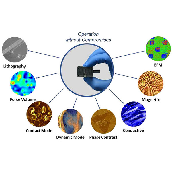
L’AFSEM™ est un microscope à force atomique capable d'effectuer tous les modes de mesure attendus d'un AFM standard. Le mode contact, le mode contact intermittent, le mode sans contact, le mode force-volume et le mode contraste de phase sont tous disponibles et l'utilisateur peut passer de l'un à l'autre facilement à l'aide du logiciel de contrôle. Les modes avancés, à savoir l'AFM à pointe conductrice (C-AFM), la microscopie à force magnétique (MFM) et la microscopie à force électrostatique (EFM) sont également disponibles en utilisant les sondes fonctionnelles. La microscopie de force à sonde Kelvin (KPFM) et la microscopie thermique à balayage (SThM) sont actuellement en cours de développement.
AFSEM nano - Introduction Video
Measurement modes:
Standard AFM
In contact mode, the tip is in contact with the surface of the sample and follows the topography closely in the repulsive regime. For contact mode long and soft cantilevers with low force constants are used.
(Figures 1 and 2) AFSEM image of a polymer surface obtained in contact mode.
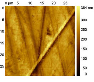
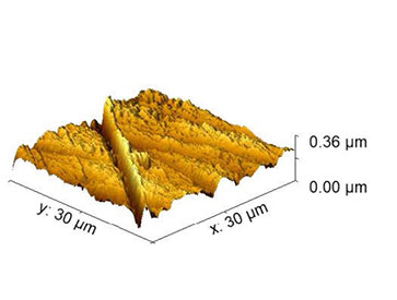
In intermittent contact mode, also called dynamic mode, the cantilever is oscillated near its resonance frequency. When the tip comes close to the surface, the interaction between the tip and the sample cause the amplitude of the oscillation to change. As the cantilever is scanning over the sample, the height is adjusted to maintain a set cantilever oscillation amplitude. An AFM image is therefore produced by imaging the force of the intermittent contacts of the tip with the surface.
AFSEM image of freestanding graphene membranes obtained in intermittent contact mode.
(Figure 1) Correlative SEM/AFM image of the graphene membranes.
(Figure 2) High-resolution AFM image of a single freestanding graphene membrane.
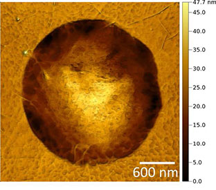
In non-contact mode, the tip of the cantilever does not contact the sample surface. The tip is oscillated only with a very small amplitude and is affected only by the long-range forces and therefore neither sample degradation nor tip degradation occur.
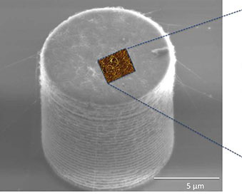
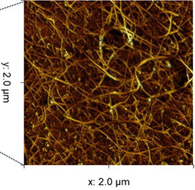
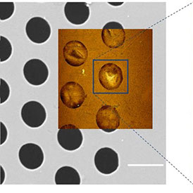
AFSEM image of silicon micro-pillar surface obtained in non-contact mode
(Figure 1) Correlative SEM/AFM image of the micro-pillar surface.
(Figure 2) High-resolution AFM image of the micro-pillar surface decorated with nano-wire network.
In force-volume mode, force measurements are combined with topographic imaging. Typical AFM images depict the topography of a surface by measuring the action of a feedback loop to maintain a constant tip/sample interaction as the tip is scanned across the surface. The force volume data set combines nearly simultaneously measured topographic and force information into a single data set allowing the microscopist to test for correlations between forces and surface features.
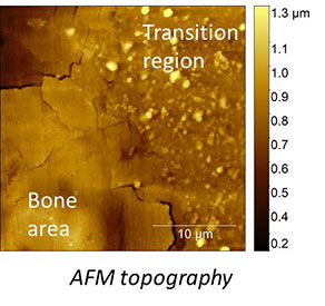
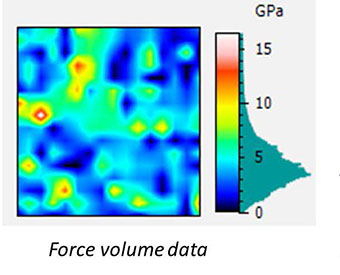
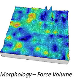
AFSEM image of bone sample with a partially dissolved implant obtained in force volume mode.
(Figure 1) AFM Topography image of the bone area and transition region, where the implant is partially dissolved.
(Figure 2) Force volume data of the same area.
(Figure 3) Overlay of topography and force volume data.
C-AFM
Conductive AFM mode (C-AFM) measures the conductive properties of the sample using a conductive tip. The conductive tips used by AFSEM are produced using Focused Electron Beam Induced Deposition (FEBID) and are made of pure Platinum, which ensures their high stability and longevity. There is no extra module needed for C-AFM measurements.
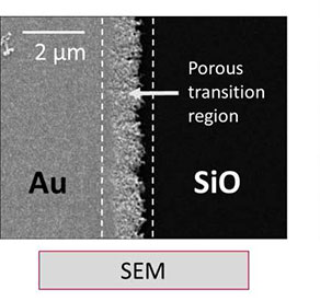
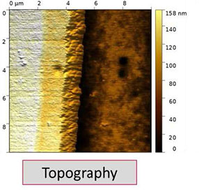
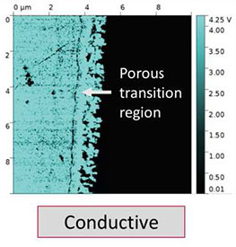
AFSEM C-AFM image of a gold electrode on a silicon substrate.
(Figure 1) SEM image of the region of interest displaying the gold electrode with a porous transition region at the edge of the electrode structure.
(Figure 2) AFM Topography image of the electrode structure.
(Figure 3) C-AFM image of the electrode structure that reveals the highly conducting gold electrode as well as the non-conducting silicon surface region.
MFM
Magnetic AFM Mode (MFM) is used to study the magnetic properties of magnetic materials using a magnetic tip. The conductive tips used by AFSEM are produced using Focused Electron Beam Induced Deposition (FEBID) and are made of Fe/Co. AFSEM uses a dual pass technique: A first scan images the topography. Then a second scan, where the tip follows the measured topography with a set distance above the sample, measures the phase shift due to magnetic force between tip and sample. By default, the AFSEM is capable of this so called "lift-mode".
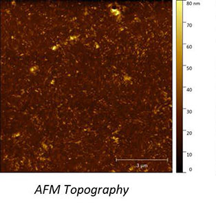
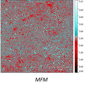
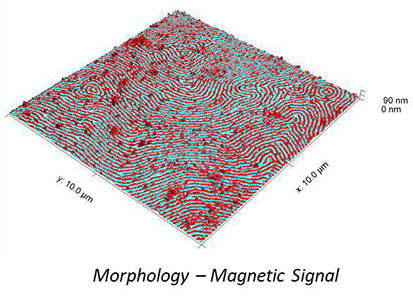
AFSEM MFM image obtained on a multilayered magnetic sample.
(Figure 1) AFM Topography.
(Figure 2) MFM Phase contrast revealing the different magnetic domains.
(Figure 3) Overlay of topography and magnetic signal.
Caractéristiques techniques
AFSEM nano is the smallest AFM isnert for your SEM/FIB. Its small size and weight enable easy-integration in extremely space-limited environments. The full grade V titanium body offers optimized mechanical stability and performance.
| Sample Limitations | Unlimited in terms of size and weight |
| Scanner Specifications |
|
| Scanner Dimensions | 61mm x 51mm x 28mm |
| Scanner Weight | 180g |
| Scan Range | 24µm x 24µm |
| HV compatibility | 1x10^(-7) |
| Positioning Stage |
|
| Travel Range | x/y/z: 12mm |
| Coarse Resolution | 100nm (minimum, user controllable) |
| High-Speed Controller |
|
| Measurement Modes | Supports all standard and advanced measurement modes modes (c-AFM, MFM, EFM, KPFM, SThM,…) |
| Input/Output | 8 channels (156 kHz, 24 bit, on demand user configurable) |
| High Voltage Amplifier | 3 high-bandwidth channels (x,y: 10 kHz, z: 300kHz) |
Téléchargements


Vidéos
Contact


Navigation
Catégories
Contact
Quantum Design S.A.R.L.
Avenue de l’Atlantique
Bâtiment Fuji Yama
91940 Les Ulis
France
| Tél. : | 01 69 19 49 49 |
| Email : | franceqd-europe.com |