In-situ MFM and SEM measurements of magnetic multilayer structures and duplex steel samples with the AFSEM
Magnetic compounds and multilayer structures are promising materials when it comes to solving problems in the fields of spintronics, thermoelectrics, nanoelectrics and information technology. Currently, these materials are mainly used in the field of data storage, and magnetic force microscopy (MFM) is one of the most commonly used analysis methods.
MFM measurements not only allow statements about quality to be made, but also local differences of the magnetic domains can be investigated down to nanometer scale. In particular, the possibility to perform these MFM measurements as correlative in-situ measurements in a scanning electron
microscope (SEM) opens completely new horizons for high-resolution analysis of magnetic structures.
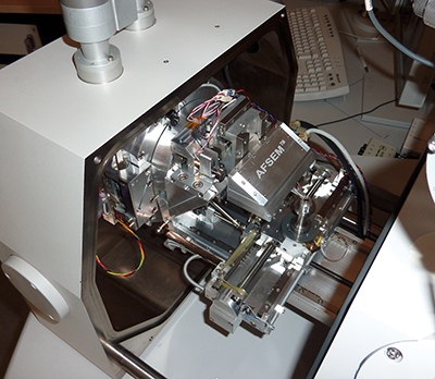
In this article, we are going to present you the results of two measurements which we carried out together with our customers and our partner GETec in their measurement laboratory in Vienna. For the MFM measurements with the AFSEM, specially fabricated MFM cantilevers were used, which were manufactured using the 3D-nanoprinting process (FEBID). They have a significantly smaller tip radius of about 10 nm as compared to conventional MFM cantilevers. In figure 1, you can see a current photo of the measurement setup. The SEM is a Quanta FEG 600 into which the AFSEM has been integrated.
The first sample is a Si/SiO substrate on top of which alternating layers of platinum and cobalt have been placed. These measurements were performed in cooperation with the Helmholtz Centre in Dresden Rosendorf. Figure 2 shows the SEM image in which the MFM cantilever and the sample surface can be seen (a), as well as the topography signal of the AFM (b) and the MFM signal (c). The high MFM contrast makes the different magnetic structures of the sample visible.
The second measurements were carried out together with TU Dortmund University. In this case, the sample is a duplex steel consisting of paramagnetic and ferromagnetic phases that are distributed over the entire surface. In Figure 3 you can see the SEM image, showing the MFM cantilever and the sample surface (a), the SEM image with an optimized contrast for gaining a first impression of the two phases (b), and a superposition of the topography image of the AFM (c) and the MFM signal (d) with the SEM image. Here, the advantage that the correlative approach of SEM and AFM offers for this sample is quite obvious.
We would like to thank Dr. L. Fallarino, Dr. G. Hlawacek, Prof. O. Hellwig, Dr. M. Knyazeva, J. Rozo Vasquez and Prof. F. Walther for providing the samples and for the good cooperation.


