Relative orientation of 2D semiconductors

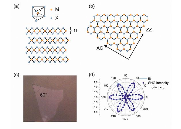
(a) Crystal structure of MX2-based transition metal dichalcogenides; (b) Monolayer crystal form of the top side with "armchair" AC and "zigzag" (ZZ) direction; (c) Optical image of a monolayer crystal with sharp edges. The angle of 60° indicates that both edges are either AC or ZZ; (d) Polarization resolved SHG TMD monolayer crystal lattices in the 2H phase belong to the trigonal-prismatic (D3h) point group
Researchers at TU Dortmund University have determined the relative orientation of atomic 2D semiconductors using "second harmonic generation". They used an Andor Technology spectrometer that consisted of a Kymera 328i spectrograph and an iDus 416 CCD detector.
Two-dimensional atomically thin materials have been studied very intensively in the past decade. Crystals with a layered structure in which strongly bonded atomic layers are held together by weak van der Waals forces can be split into single layers by mechanical exfoliation. Transition metal dichalcogenides with the chemical formula MX2 consist of transition metals M of group IV, V or VI (e.g. Ti, V, Mo) and chalcogenide atoms X (S, Se, Te). Monolayers of these materials have unique properties that differ greatly from the corresponding bulk or multilayer form. Controlled stacking of individual layers of the same or different material makes it possible, e.g., to manipulate optical and electrical properties. However, stacking two monolayers with precise alignment of the crystallographic axes requires a method to measure their relative orientation. Although the crystals break along specific crystal axes, an optical image does not allow a distinction to be made between them.


