Watching carbon layer growth at elevated temperatures in real time

More and more, the so-called “bottom-up” method is used in the manufacturing of electronic and optical components. This means, functional materials are build up atom by atom for optimal customization.
Typical examples are heterostructured semiconductors like nanowires, carbon nanotubes or graphene with tailored bandgaps and high electron mobility.
The synthesis of such materials is highly sensitive to parameters like temperature, utilized precursors and experiment duration. And the contained structures and morphologies determine the macroscopic properties like resistance, electrical, magnetic and optical behavior, catalytic performance and more.
To synthesize customized materials for specific applications, the material’s reaction behavior needs to be thoroughly understood. In situ TEM experiments for real time observation allow insights into chemical processes on the atomic level.

Fig. 1a to d: Time-resolved carbon layer growth by vapor deposition on nickel at 650 °C. Arrows indicate the growth front.
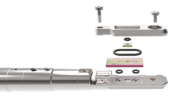
The Climate TEM instruments allow the introduction of gas into a reaction chamber (nano reactor) at elevated temperatures. Experiments showed the carbon layer growth from vapor deposition (CVD) on a nickel catalyst. First, nickel was deposited on a MEMS chip and heated to 650°C under hydrogen atmosphere. Then C2H2 (acetylene) was introduced as precursor. The highly resolved TEM analysis showed layered growth of carbon structures on the boundary layers of nickel and carbon. Figures 1a to d show the growth of carbon layers on the nickel catalyst, time-resolved and observed in situ.
The Climate series will soon be available for transmission electron microscopes from FEI and JEOL.
Contact
| +49 6157 80710-557 | |
| +49 6157 807109557 | |
| Write e-mail |


