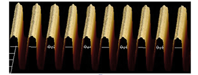
Nano Imprint Lithography
In addition to the well-established photo lithography for the production of polarizers, Moxtek now offers state-of-the-art NIL volume production on 8-inch glass and silicon wafers. Nanoimprint lithography (NIL) is a nanolithography method for the cost-effective production of nanostructures with a resolution below the diffraction limit. The desired structure is stamped into a positive that is heated above the glass temperature. The structure is then transferred to the substrate by etching.
Data from 10,000 processed wafers shows that the stamps reach a lifetime of 500 to 750 prints, in some tests even up to 1,300 prints. Throughout this time, they comply with the critical dimension (CD) of 30 nm. Moxtek’s service covers the entire production process from master design and manufacturing, stamp production, prototyping of imprints to mass production.
In addition, Moxtek offers DoE and leaning cycles for print optimization to-
gether with Statistical Process Control (SPC) to monitor the repeatability of the CD after printing.
The NIL process is ideally suited for cost-effective mass production of functional micro- and nanostructures. Applications include waveguides, diffractive optics, microlens arrays, photonic crystals and other meta-surfaces in display, imaging, AR/MR, medical and automotive technology.
Further information can be found in a Moxtek White Paper.
Contact
| +49 6157 80710-34 | |
| +49 6157 80710934 | |
| Write e-mail |

| +49 6157 80710-15 | |
| +49 6157 80710915 | |
| Write e-mail |


