Fast non-destructive 3D analysis for advanced packaging and semiconductors
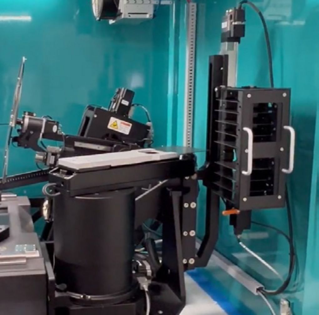
Apex Hybrid from SigrayThe Apex Hybrid from Sigray combines laminography and tomography in a single X-ray microscope, enabling fast, precise and non-destructive analysis of modern semiconductor and packaging structures.
With a spatial resolution down to 350 nm and the patented Precision Angle Laminography (PAL) geometry, the system delivers high-resolution 3D images even for large, intact samples such as 300 mm wafers, panels or printed circuit boards.
- Dual-mode imaging: laminography and tomography in one system
- 350 nm spatial resolution with high throughput
- Patented PAL geometry for artifact-free 3D imaging
- Open nanofocus X-ray source with automatic calibration
- Fully automated sample handling and GPU-accelerated reconstruction
- Ideal for advanced packaging, TSVs, RDLs, microbumps and hybrid bonds
Further information
As electronic devices become smaller and more complex, inspection challenges in advanced packaging increase dramatically. Traditional computed tomography (CT) struggles with large, flat samples such as wafers or printed circuit boards, while conventional laminography suffers from incomplete data and reconstruction artifacts.
The Sigray Apex Hybrid solves these issues with a dual-mode design that merges laminography and tomography within a single compact system. This approach allows users to capture both macro-scale overviews and submicron details — without switching instruments or repositioning samples.
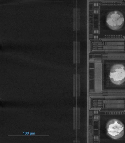
Representative X-ray view of advanced packaging structures (scale: 100 µm).
Precision Angle Laminography (PAL)
Sigray’s patented Precision Angle Laminography (PAL) provides exceptional image clarity by minimizing the “missing-cone” problem of traditional laminography. With shallow projection angles between 10° and 20° and an ultra-stable air-bearing rotation, PAL delivers artifact-free visualization of critical vertical features such as through-silicon vias (TSVs), microbumps, and redistribution layers (RDLs).
Dual-mode flexibility
In laminography mode, users can rapidly inspect large or fully assembled boards, panels, or wafers. For regions requiring higher detail, the system seamlessly switches to tomography mode, achieving up to 350 nm spatial resolution. This hybrid workflow saves preparation time and enhances efficiency in both R&D and production environments.
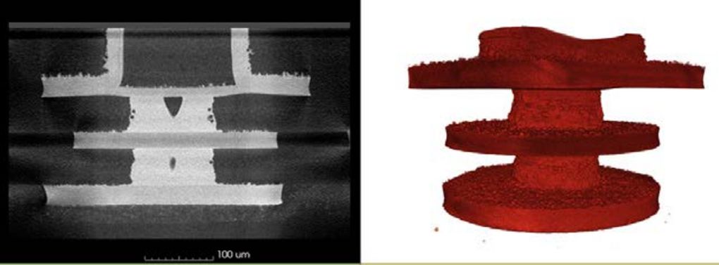
Dual-mode workflow from overview to high-resolution 3D reconstruction (scale: 100 µm).
High-performance X-ray source and calibration
The Apex Hybrid features an open transmission X-ray source with a tungsten-on-diamond target. Internal calibration patterns automatically measure the effective focal spot for every scan, ensuring metrological accuracy and consistency over long operation periods. Compared with sealed-tube sources, the open design offers extended lifetime and significantly lower maintenance costs.
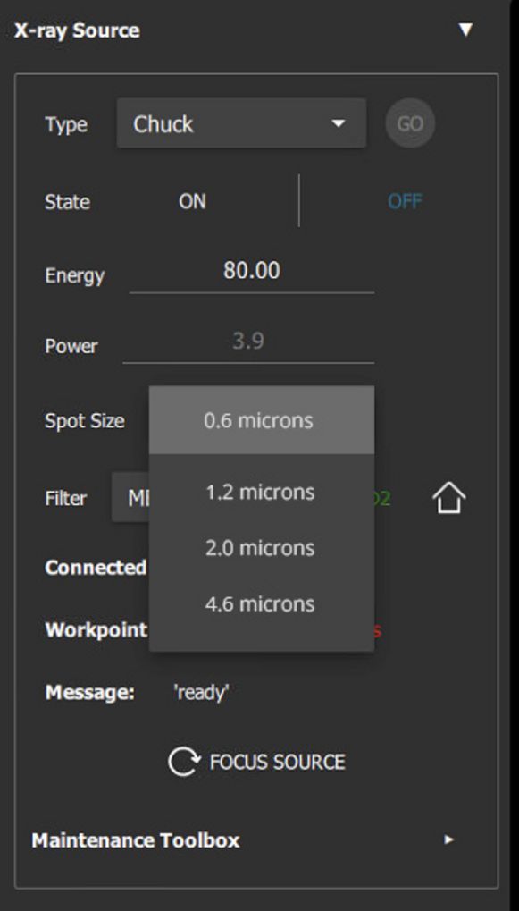
Internal calibration and spot-size control ensure metrologically consistent imaging.
Automation and detector options
For laboratories with high sample throughput, the Apex Hybrid can be configured with an in-system sample robot capable of handling up to ten 100 × 100 mm samples automatically. Users can select between several detector options: HyperCapture (7 MP), HyperCapture-XL (13 MP) or UltraVision (16 MP). Sigray’s optional MegaView montage module combines multiple scans into a seamless, large-scale 3D dataset for complete inspection of printed circuit boards or complex packages.
Automation-ready design with in-system sample robot for unattended operation.

Sigray’s software provides multi-view visualization and analysis of 3D datasets.
Why choose Apex Hybrid
- Two imaging systems in one: laminography and tomography combined for unmatched flexibility.
- Exceptional clarity: PAL geometry eliminates common laminography artifacts.
- Submicron precision: 350 nm spatial resolution with internally calibrated X-ray source.
- Automation-ready: robotic handling and scripting via Python API streamline workflows.
- Scalable and future-proof: ideal for semiconductors, advanced packaging, batteries, and materials science.
Specifications
| Parameter | Specification |
| Spatial resolution | 350 nm (voxel < 100 nm) |
| Imaging modes | Laminography / Computed Tomography |
| Maximum sample size | Laminography: 300 mm wafer / 213 × 213 mm panel CT: 150 × 150 mm |
| Stage travel (XYZ) | 100 × 20 × 100 mm |
| X-ray source | Open transmission source, tungsten-on-diamond (40–160 kV / 16 W) |
| Detectors | 6.7 MP / 13 MP / 16 MP (UltraVision option) |
| Software | XRM Companion · GigaRecon · Sigray 3D Viewer · Python API |
| Typical applications | Advanced packaging · Microbumps · TSVs · Batteries · Reverse engineering |
Applications
The Apex Hybrid is designed for industries where precision, reliability, and throughput are essential. Its dual-mode architecture supports a wide range of applications, from advanced packaging to materials research.
- Advanced packaging: detailed 3D inspection of TSVs, RDLs, microbumps, and hybrid bonds.
- Failure analysis: rapid detection and localization of hidden defects in semiconductor assemblies.
- Reverse engineering: non-destructive structural analysis of PCBs, ICs, and multi-chip modules.
- Battery research: visualization of internal electrode structures and degradation over time.
- Materials science: high-resolution imaging of composites, ceramics, and microstructured materials.
With its combination of imaging flexibility, automation, and precision, the Apex Hybrid provides a single platform to accelerate innovation across R&D and production environments.
Downloads

Contact

Navigation
Categories
Contact
Quantum Design s.r.l.
Via di Grotta Perfetta, 643
00142 Roma
Italy
| Phone: | +39 06 5004204 |
| Fax: | +39 06 5010389 |
| E-mail: | italy@qd-europe.com |