
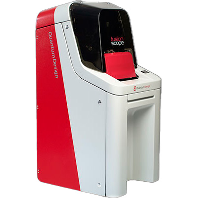
Correlative Microscopy Platform for AFM, SEM, EDS and Nanoprobing – FusionScope
FusionScope from Quantum DesignCorrelative Microscopy with the FusionScope
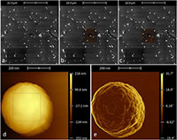
The FusionScope is a microscopy platform for correlative analysis, combining multiple high-resolution techniques in a single instrument: Atomic Force Microscopy (AFM) and Scanning Electron Microscopy (SEM), with Energy Dispersive Spectroscopy (EDS) and Nanoprobing available as optional methods. Thanks to a shared coordinate system across all techniques, complementary data from the same region can be directly viewed in context, revealing how the information provided by different imaging techniques is interrelated. This correlative approach opens up possibilities for deeper insights and a more comprehensive understanding of materials, nanostructures, electronic devices and surfaces.
- Correlation of microscopy data
- SEM for ultrafast identification of structures for AFM
- High-precision AFM navigation with SEM in 3D
- One instrument → no sample transfer
Further information
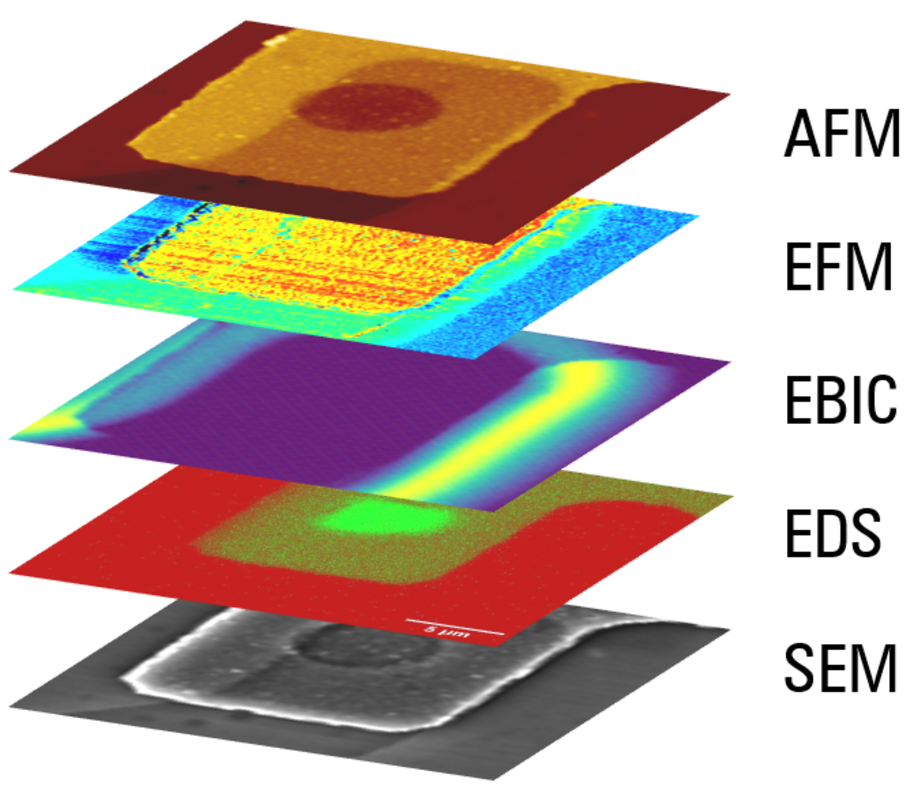
Correlation of microscopy data
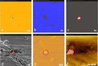
- e.g., EDS & AFM: Correlate chemical information with roughness, conductivity, and mechanical properties
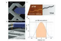
- e.g., SEM & AFM: Distinguish surface vs. subsurface features with AFM data
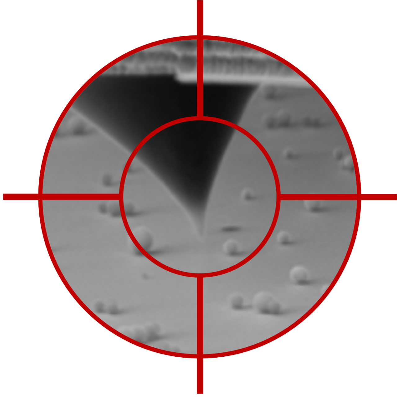
Use SEM for ultrafast identification of structures for AFM
- Targeted particle analysis
- Precise fiber detection and characterization
- Rapid nanostructure localization and investigation
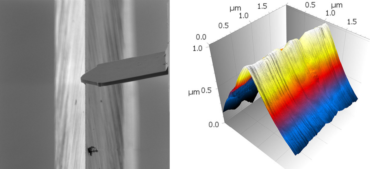
High-precision AFM navigation with SEM in 3D
Up to 80° tilt with Profile View
- Effortless AFM on corrugated samples
- Easy access to hard-to-reach regions
- Live monitoring and verification of AFM measurements
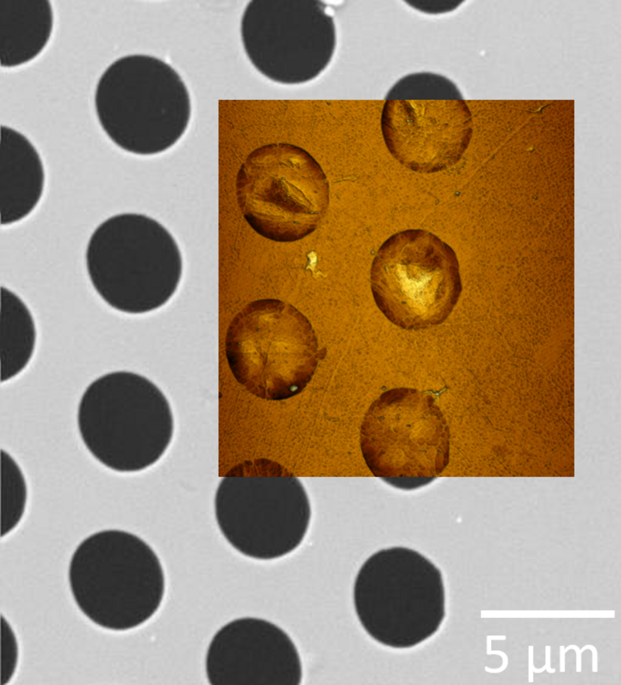
One instrument → no sample transfer → full control
- Eliminates the need to relocate measurement regions
- Saves instrument and operator time
- Prevents sample contamination or alteration
Available Microscopy & Analysis Modes
Atomic Force Microscopy (AFM)
- Contact Mode
- Dynamic Mode (Tapping)
- Force-Distance Curves
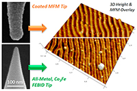
- Magnetic Force Microscopy (MFM)
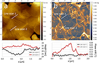
- Electrostatic Force Microscopy (EFM)
- Conductive AFM (C-AFM)
- FIRE Mode
Scanning Electron Microscopy (SEM)
- Secondary Electron (SE) Imaging
Energy Dispersive Spectroscopy (EDS)
- Elemental Analysis
- Spectrum Acquisition
- Elemental Mapping
Nanoprobing
- Voltage Biasing for I-V Curves, EFM and C-AFM
- Electron Beam Induced Current (EBIC)
- Electron Beam Absorbed Current (EBAC)
FusionScope Software
FusionScope provides a unified software environment for AFM, SEM and EDS. Measurements from the different techniques can be correlated within the shared coordinate system, while integrated workflows support efficient navigation, measurement and analysis.
Specifications
AFM
| Parameter | Specification |
| XY Scan Range | 22 × 22 µm (closed loop) |
| Z Scan Range | 11 µm |
| Imaging Noise | <50 pm at 1 kHz |
| Cantilever Probes | Self-sensing piezoresistive |
SEM
| Parameter | Specification |
| Electron Source | Thermal field emission |
| Acceleration Voltage | 3.5–15 kV |
| Probe Current | 5 pA–2.5 nA (300 pA typical) |
| Magnification | 25×–200,000× |
| Detector | In-chamber Everhart-Thornley secondary-electron detector |
EDS Option
| Parameter | Specification |
| System Resolution | <133 eV at Mn-Kα @ 14 kcps @ 1 µs peaking time |
| Detection Range | Carbon–Uranium |
| Spectrum Mode | Yes |
| Elemental Mapping | Yes |
| Detector Type | Silicon drift detector (SDD) |
Sample and Chamber
| Parameter | Specification |
| Maximum Sample Diameter | 20 mm (12 mm Full Correlated Mode) |
| Maximum Sample Height | 20 mm |
| Maximum Sample Weight | 500 g |
| Eucentric Alignment | Automatic |
| Typical Chamber Vacuum | 10-4–10-5 mbar |
| Pumping Time | <5 min |
| Trunnion Tilt | -10° to 80° |
System
| Parameter | Specification |
| Power | AC: 200–230 V; 50/60 Hz; Single Phase; 15 A |
| Dimensions (W × L × H) | 690 × 835 × 1470 mm |
| Weight | 330 kg |
Applications
FusionScope supports correlative microscopy across a broad range of research and analytical applications, including:
- Nanostructures
- Nanoparticles
- Coatings
- Semiconductors
- Batteries
- Pharmaceuticals
- Materials Science
- Quality Control
- Failure Analysis
Downloads
General Information

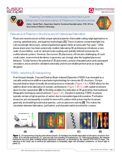
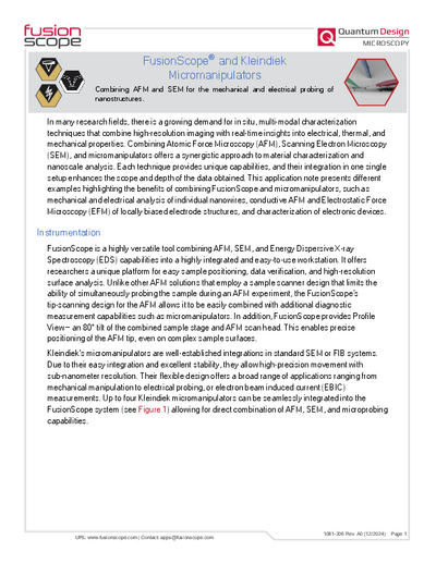
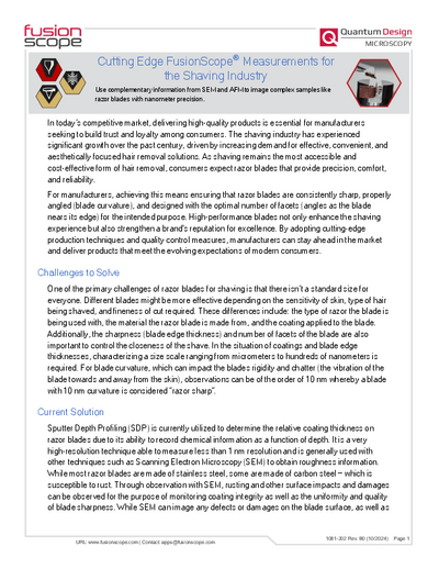
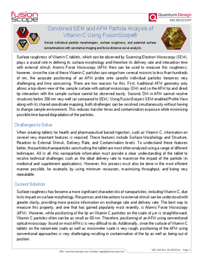
Application Notes
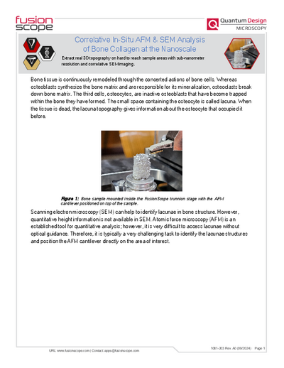
Videos
Publications
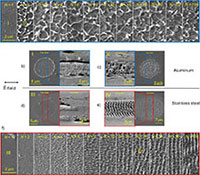
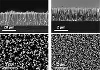
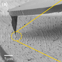


Contact

Navigation
Categories
Contact
Quantum Design GmbH
ul. Sztygarska 12/3
41-500 Chorzow
Poland
| Mobile: | +48 515 166893 |
| E-mail: | polandqd-europe.com |
Support