Scanning Microwave Microscopy (SMM)
Over the last few decades, the drive to miniaturize electronics has increased the demand for nano-electrical characterization methods. Understanding the local electronic material properties, such as conductance, dielectric constant, local capacitance and dopant density is critical for research and development of the semiconductor and microelectronics industries.
Atomic force microscopy (AFM) has been a key technology used to correlate topographical structures with local electronic properties at the nanoscale. Techniques such as conductive atomic force microscopy (CAFM) and Kelvin probe force microscopy (KPFM) allow for the measurements of local currents and electric surface potentials while scanning capacitance microscopy (SCM) maps the capacitance or local carrier density. Scanning microwave microscopy (SMM) is unique in revealing buried structures that are prevalent in multilayered modern integrated circuits (ICs).
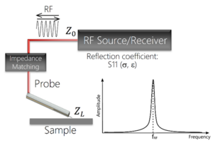 Scanning Microwave Microscopy (SMM) is a scanning probe technique, that measures the interactions of a microwave from a sharp tip with the sample. The microwave reflection coefficient (S11 parameter), which is the ratio between the microwave power sent to the tip and the one received back after being reflected at the tip-sample contact, is used to deduce the local tip-sample microwave impedance. The microwave impedance yields information about the local capacitance from which one can deduce the dielectric constant and the dopant density. In terms of the dopant density measurement, the SMM is similar to the Scanning Capacitance Microscopy (SCM), but offers wider range of measurements. SMM can be used for measurements of not only semiconductors, but also dielectric materials and metals, since it is not solely relying on the modulation of the depletion capacitance in the sample.
In semiconductor materials, an AC voltage bias can modulate the dopant density in the sample under the tip, and therefore the S11 signal. This is called the dS/dV measurement, which yields similar information to the conventional dC/dV measurement in SCM. The dS/dV is less affected by topography, but it only works for semiconductors. Another advantage of this method is that it yields information about the type of the dopants via phase change.
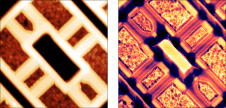
As an example see below the topography (left) and Im(S11) or capacitance (right) of a SRAM sample (Scan size is 10 x 10 μm2) that exhibits structures with clear differences in dopant type and concentration. From the SMM measurement device faults or relative changes in dopant concentration could be identified to evaluate device performance or potential sites for failure.
Click here to read the App Note "Scanning Microwave Microscopy (SMM)" >>>
Calibration of capacitance and/or dopant density measurements
While it is possible to extract the sample local electronic parameters from the SMM measurement purely by analytical methods, the calculations require precise knowledge about the sample parameters and are computationally extensive. In semiconductors it is also necessary to know which model for the carrier mobility to use. In practice, a much faster way to obtain quantitative data is calibrating the measurements on known standards.
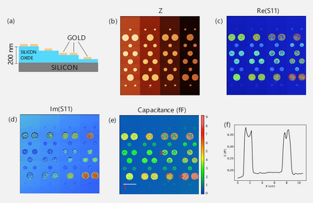
Below we report an example of calibration of S11 measurement of the MC2 Technology capacitance calibration sample. (a) Sample schematics showing 4 terraces, each 50 nm high, with patterned golden dots on top to be used as capacitance standard. (b) Topography of the sample, measured in contact mode, scan size: 52 x 52 μm2. (c,d) Images of real and imaginary parts of S11 parameter. (e) Capacitance image, recalculated from the S11 parameter. Capacitors indicated with numbers 1, 2 and 3 were selected as calibration standards. Their respective capacitances were theoretically estimated as 0.3, 3.6 and 12.4 fF. These values vere used to calculate the capacitance map. (f) Cross section along the white line in (e), showing the contrast of a scan over two smallest capacitors. The smallest capacitance change in the image, the step between the terraces, is 0.04 fF.
Below we report the experimental data of the S11 (b,c) and dS/dV (d,e) measurements of the Infineon SCM calibration standard sample. The area consists of 20 regions with different doping: 10 for each dopant type (n and p) with dopant densities in the range 4⋅1015 - 1020 cm-3 The difference between the S11 and dS/dV can be clearly seen. The amplitude of S11 signal (b) is monotonically increasing with the carrier density, while the dS/dV signal (d) has largest amplitude in the middle of the range (1016-1018 cm-3). Phase signal of the dS/dV carries information about the type of dopants, n or p. The doping profile (f) was calculated from the S11 measurement (b,c). Image size (a,b,c,f): 50 x 50 μm2, (d,e): 35 x 35 μm2.

Check our range of AFMs >>>
| +39 06 5004204 | |
| +39 06 5010389 | |
| pergoliniqd-europe.com |