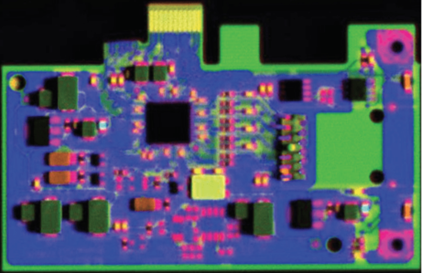
Semiconductors testing with ATLAS micro-XRF system
Rapid elemental analyses from sodium through uranium at trace levels can be accomplished through X-Ray Fluorescence (XRF) instrumentation without destruction, digestion, or alteration of the sample. The innovative benchtop micro-XRF ATLAS system by iXRF Systems is ideally suited for the analysis of inorganic species and offers excellent sensitivity to trace elements (concentrations of less than 100 ppm can be detected, depending on the element and sample matrix). No sample preparation is needed: highly polished samples are not required, and even rough samples can be analyzed with excellent results.
Non-destructive tests (NDTs) are a must have methods to improve the quality control of manufactured products. As it stands, electronic components are present everywhere in our modern world and it is imperative that these components must be reliable. To assure this reliability, components must go through an NDT protocol: XRF analysis is an irreplaceable tool for the semiconductor industry, not only to guarantee their reliability, but to also assure their correct compliance. Electrical or photonic circuits are the foundation for so many other products, beginning their lives on silicon wafers. As the wafers and associated circuits and boards become more specialized, they require different types of testing.
The ATLAS system has the largest sample chamber on the market, which can easily map up to a 300 mm wafer with high resolution, up to 5 µm. Its applications range goes from metal nanoparticle contamination to thin film/coating thickness measurements (metrology) and many more.
For example, there is a well-known phenomenon, known as ‘whiskers’ that can cause electronic components to fail. These whiskers come from tin used in electronic component surfaces and it has been found that adding lead to the tin can prevent the growth of whiskers. Most aerospace companies require a minimum of 3% Pb to prevent tin whiskers. Lead spots are often detectable around the SnPb solders of a circuit, which are the most common type of solders in the electronic circuits industry. However, this addition of lead must be regulated according to the expected and required concentrations, assuring, as much as possible, the final product compliance.
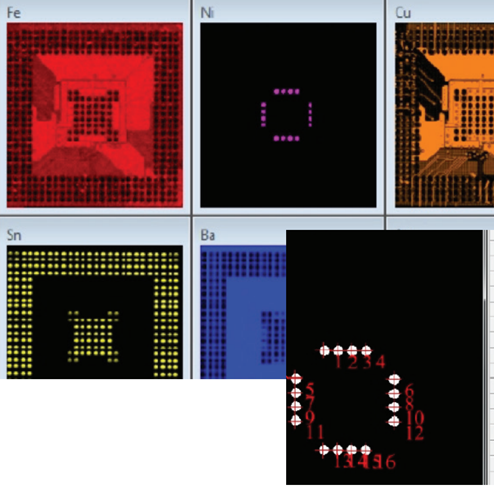
Quantitative micro-XRF mapping analysis on the SnPb solder bumps
ATLAS system’s powerful software can be used to quickly identify, measure, and analyze multiple solder bumps on a board, as well as the Pb and other metals contamination which can influence the correct functioning of the devices.
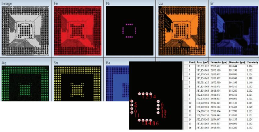
X-Ray map element overlay for an integrated circuit, including Cu, Br, Ti, Ca, Fe, Sn, Zn, Ni and Pb