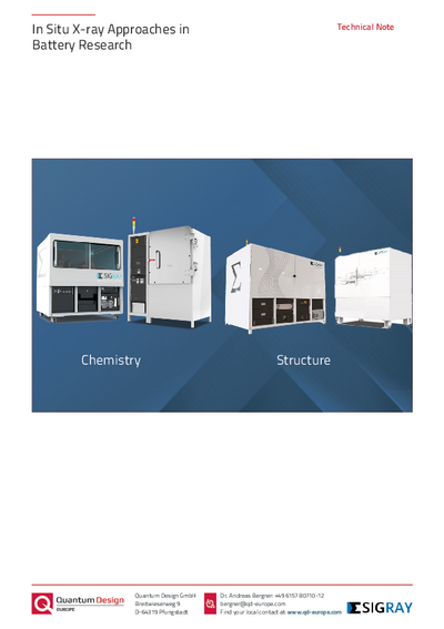
AttoMap™ - µXRF analytical microscope
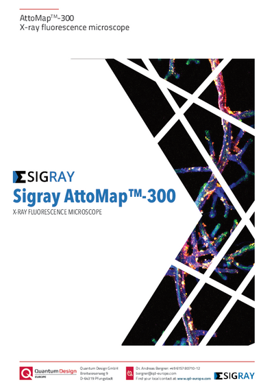
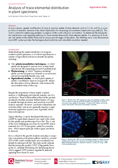
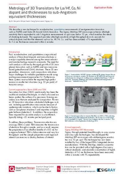
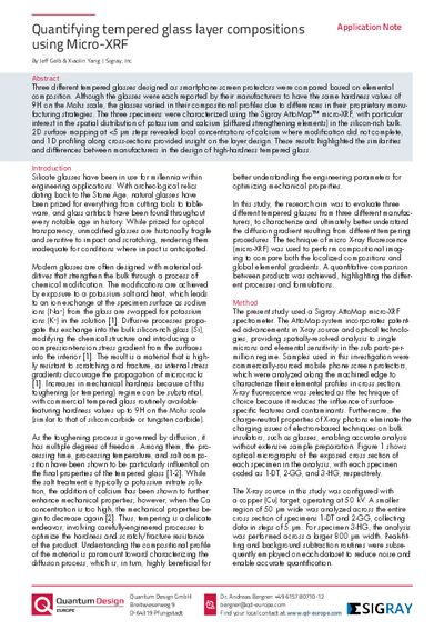
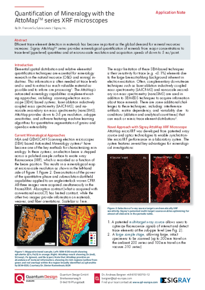
from SIGRAYThe AttoMap™ x-ray analytical microscope offers the highest resolution and the highest sensitivity one can find in a laboratory based microXRF system. The AttoMap™ system can be used for transmission-based x-ray structural analysis as well as for fluorescence chemical mapping. The system has a chemical sensitivity of <1-10 ppm for trace element analysis and the measuring time is within 1 second.
Further information
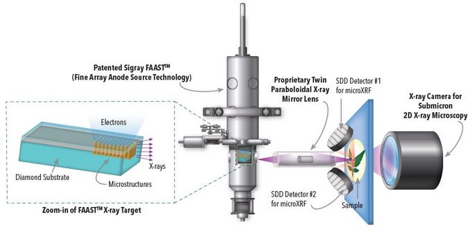
The key advantages of the AttoMap™ system compared to standard µXRF systems are three major innovations developed by Sigray.
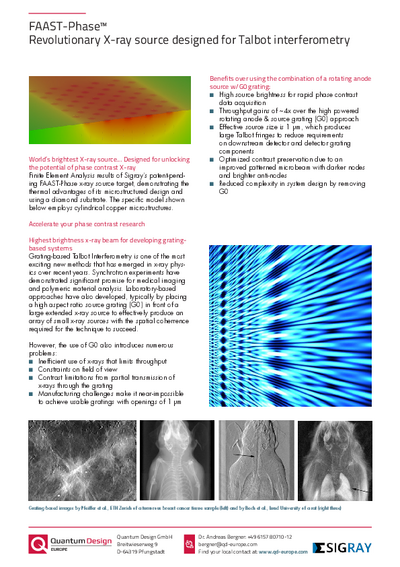
- The patented FAAST™ x-ray source with 50X higher brightness than microfocus sources used in standard microXRFs
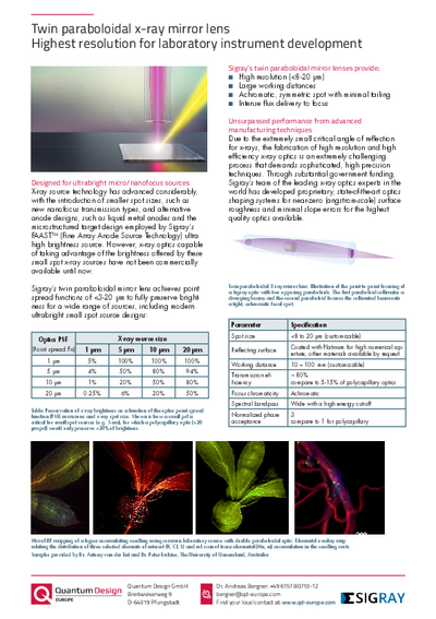
- Proprietary, high efficiency x-ray mirror lens that provides a combination of small achromatic focus and large working distance for superior detection sensitivity and accuracy
- Unique detector geometry enabled by the design of the x-ray mirror lens that collects 10X more fluorescence x-rays than conventional designs.
These innovations provide the AttoMap™ with the ultimate laboratory microXRF performance:
- Substantially higher resolution at single digit microns-scale (e.g. 3-5 µm MTF) resolution versus conventional microXRF
- Detectability of nanoparticles down to 50-100 nm
- Dramatically faster analytical speed of a single minute - rather than a half day - for equivalent measurements on an AttoMap™ versus a conventional microXRF with up to 500X higher throughput
- Sub-ppm and sub-femtogram sensitivity in seconds
- >100X the sensitivity of standard microXRF
- Only microXRF that can map trace elements (conventional microXRF is capable of mapping only major constituents at reasonable throughputs, as it requires long spot acquisition times for trace elements)
- Most accurate quantification capabilities and optional dual energy source for maximum flexibility
- Ability to analyze buried microfeatures
Models
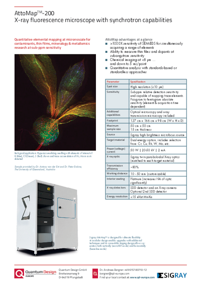
AttoMap-200
| Parameter | Specification |
|---|---|
| Spot Size | High Res (<8 µm) | Med Res additional optics also available |
| Sensitivity | Sub-ppm relative detection sensitivity and capable of mapping trace elements. Picogram to femtogram absolute sensitvity (element & acquisition time dependent) |
| Additional Capabilities & Modules | 2D correlative x-ray imaging at <1 µm resolution included (standard) Optical microscopy included (standard) Future modules will be available as upgrades |
| Footprint | 54” W x 65.5” H x 38.5” D |
| Maximum Sample Size | 50 cm x 50 cm | 15 cm thickness |
| Source | Sigray FAAST™ Microstructured Source |
| Target Material | Dual Energy Option, includes selection from: Ti, Cu, Rh, W, Pt, Zr, etc. Custom target options include materials that have previously not been used in conventional sources. |
| Power | Voltage | Current | 50 W | 20-50 kV | 4 mA |
| X-ray Optic | Sigray Twin Paraboloidal X-ray Mirror Lens |
| Transmission Efficiency | ~80% |
| Working Distance | 10 - 50 mm (customizable) |
| Interior Coating | Platinum (increases NA of optic significantly) |
| X-ray Detectors | Two SDD detectors and an X-ray Camera |
| Energy Resolution | <135 eV at Mn-Ka |
AttoMap-300
| Parameter | Specification |
|---|---|
| Spot Size | High Res (<8 µm) |
| Sensitivity | Sub-ppm relative detection sensitivity and capable of mapping trace elements. Picogram to femtogram absolute sensitvity (element & acquisition time dependent) |
| Additional Capabilities & Modules | Optical microscopy and x-ray transmission microscopy included |
| Footprint | 54” W x 65.5” H x 38.5” D |
| Stage Travel | 100 x 100 mm (upgrades available upon request) |
| Maximum Sample Size | 100 x 100 mm standard operation, ~30 x 30 mm at grazing angles | 20 mm thickness |
| Source | Sigray Patented High Brightness Microfocus Source |
| Target Material | Multiple x-ray targets (up to 4) includes selection from: SiC, Cr, Cu, Rh, W, Mo, Au, etc. |
| Power | Voltage | Current | 50 W | 20-50 kV | 2 mA |
| X-ray Optic | Sigray Twin Paraboloidal X-ray Optics (matched to each target material) |
| Transmission Efficiency | ~80% |
| Magnification | 1:1 Magnification Default; Demagnifying optics for higher resolution available upon request |
| Interior Coating | Platinum ((increases collection efficiency of optic significantly)) |
| Energy Resolution | <129 eV at Mn-Ka | <=136 eV at 5.9 keV |
Downloads
Contact
Dr.
Andreas
Bergner
Product Manager - Electron microscopy & nanotechnology
| +49 6157 80710-12 | |
| +49 6157 80710912 | |
| Write e-mail |

Dr.
Andreas
Bergner
Navigation
Categories
Contact
Quantum Design GmbH
Breitwieserweg 9
64319 Pfungstadt
Germany
| Phone: | +49 6157 80710-0 |
| E-mail: | germanyqd-europe.com |


