
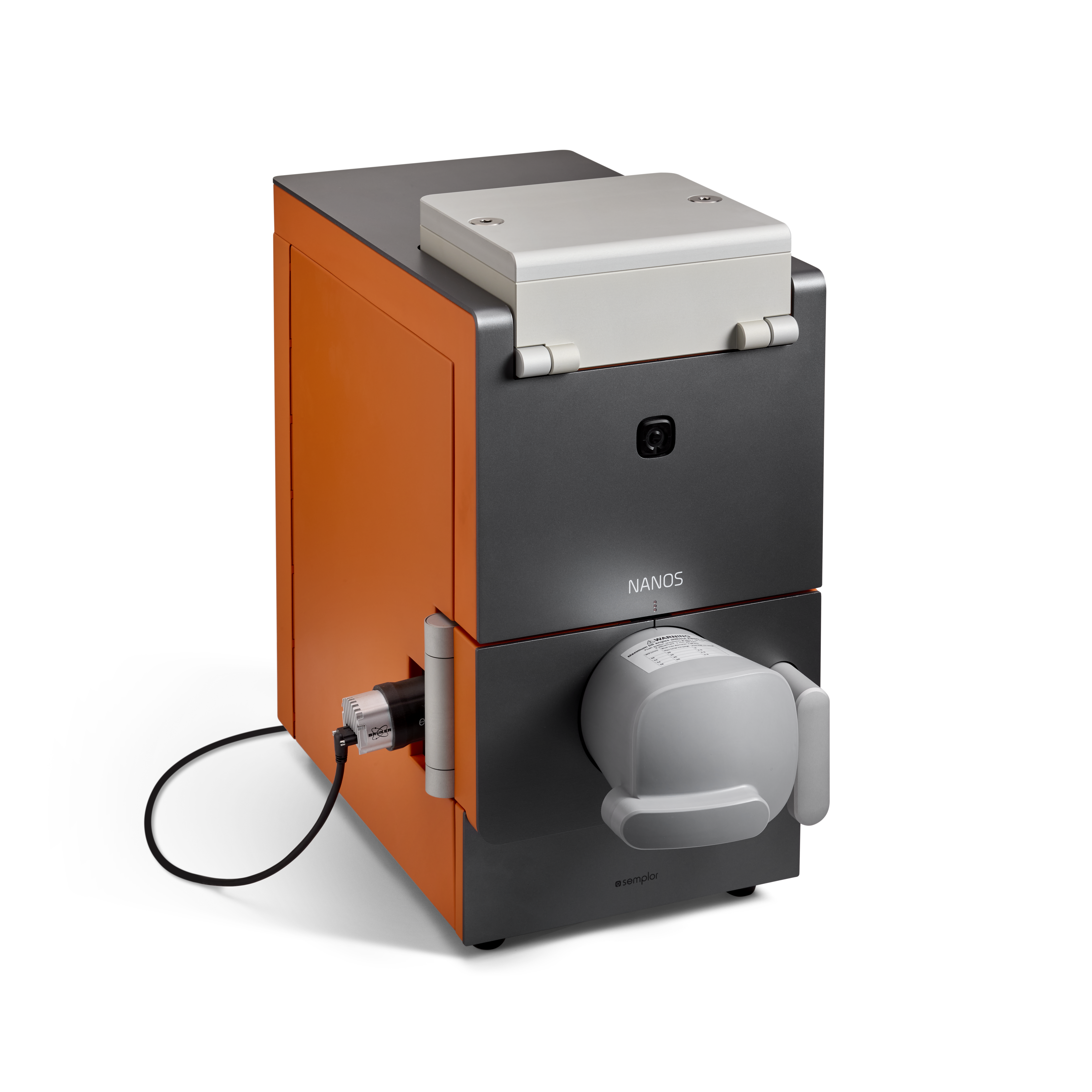

Desktop Scanning Electron Microscope for Crystallographic Analysis – NANOS EBSD
NANOS EBSD by SemplorThe NANOS EBSD by Semplor combines high-resolution scanning electron microscopy an elemental analysis (EDS)with electron backscatter diffraction (EBSD) in a compact desktop system. It provides crystallographic information such as crystal orientation, phase and grain structure while retaining the imaging capabilities of the NANOS platform. A eucentric sample stage enables a smooth transition from SEM imaging to the 70° EBSD measurement position while keeping the selected region of interest centered and in focus. Complementary EDS analysis adds information about the elemental composition of the sample.
- SEM resolution < 8 nm and magnification from 100x to 200,000x
- Integrated Bruker e-Flash XS detector for crystallographic EBSD analysis
- Crystal orientation mapping, phase identification and grain structure analysis
- Eucentric tilt between the imaging position and the 70° EBSD position
- Bruker ESPRIT software for orientation, grain boundary and texture analysis
- Compact platform for SEM imaging, EBSD and complementary EDS analysis
Further information
Electron Backscatter Diffraction for Crystallographic Analysis
Electron backscatter diffraction (EBSD) extends SEM imaging with crystallographic information about the sample. By analyzing electron diffraction patterns, the NANOS EBSD can determine crystal orientation, identify crystalline phases and characterize grain structure. This makes it possible to move beyond surface morphology and compositional contrast and investigate the crystallographic organization of a material.
Orientation mapping across the sample provides spatially resolved information about the local crystal structure. The resulting data can be used to analyze grain orientation, phase distribution and microstructural relationships within crystalline materials.

EBSD orientation map showing the crystallographic orientation of individual regions.
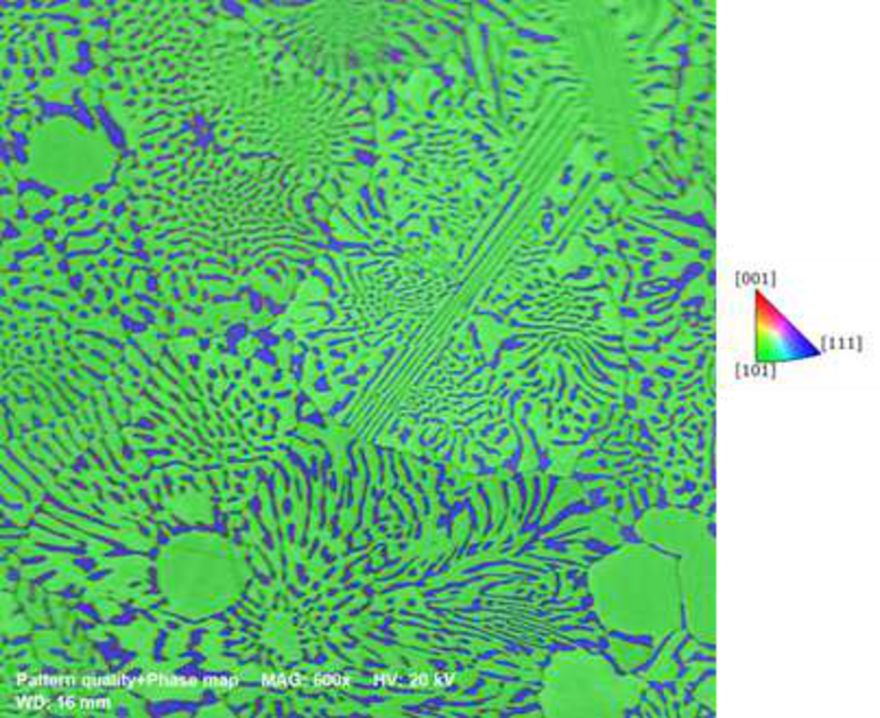
EBSD phase map for identifying and distinguishing crystalline phases.
Eucentric Tilt for a Seamless EBSD Workflow
EBSD measurements require the sample to be tilted to the measurement position. The NANOS EBSD uses a eucentric stage that allows the sample to move between the standard SEM imaging position and the 70° EBSD position while keeping the selected region of interest centered.
Because the field of view, working distance and focus are maintained during tilting, an area identified during SEM imaging can be transferred directly into the EBSD measurement position without breaking vacuum or manually repositioning the sample. This simplifies the transition from imaging to crystallographic analysis and supports a reproducible workflow.
Bruker e-Flash XS EBSD Detector
The NANOS EBSD integrates a Bruker e-Flash XS detector for fast acquisition of electron backscatter diffraction patterns. The CMOS-based detector provides a native image resolution of 720 × 540 pixels and supports multiple binning modes from 2 × 2 to 6 × 6. Pattern acquisition is possible at up to 520 frames per second across all binning modes.
A dedicated optical system with field lens maximizes light efficiency at the phosphor screen. The detector is connected via USB 3.0 for data and power transfer and works with the external QUANTAX scan generator as part of the EBSD measurement setup.
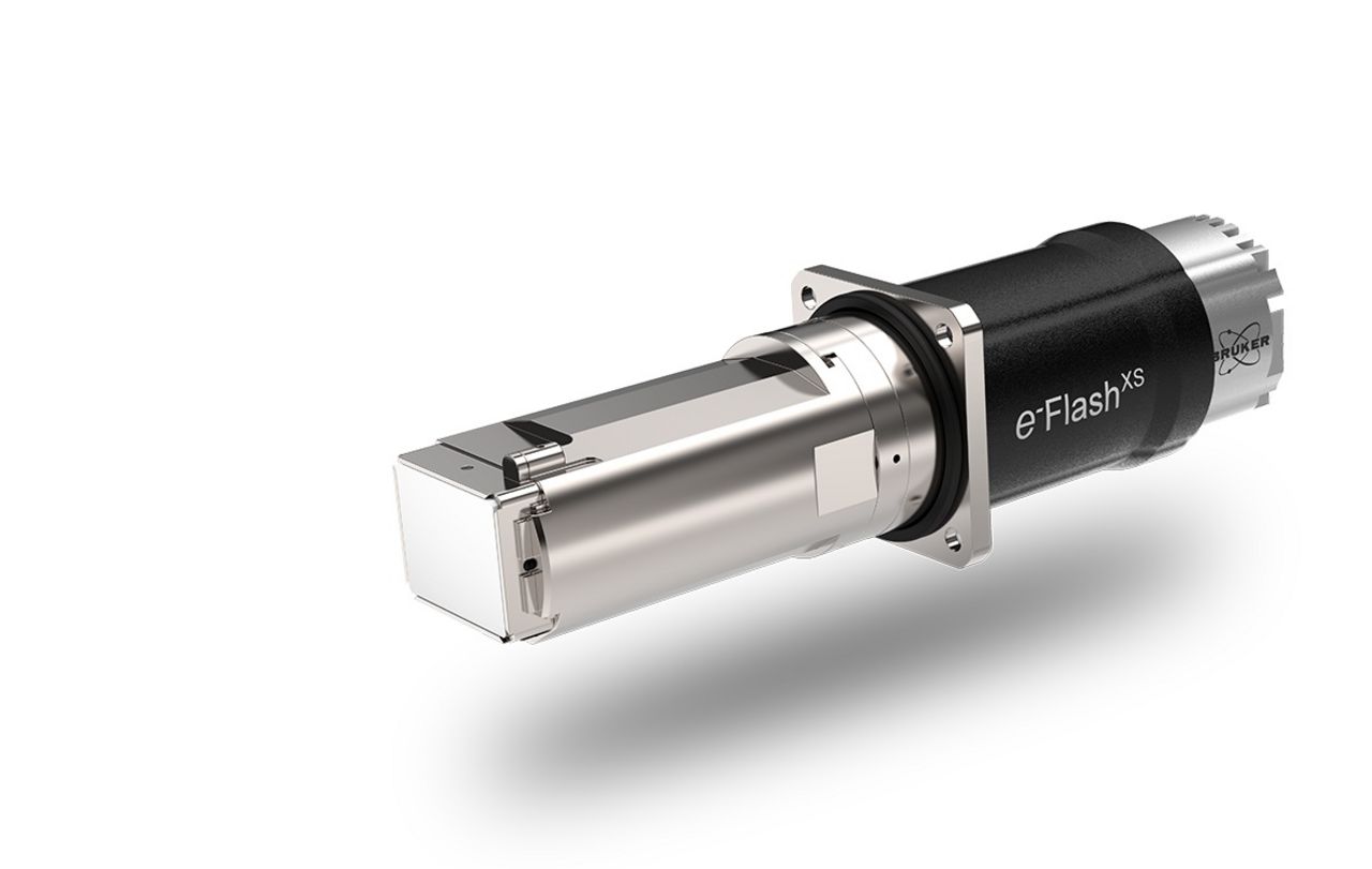
Bruker e-Flash XS detector for electron backscatter diffraction.
Crystallographic Analysis with Bruker ESPRIT
Bruker ESPRIT provides the software environment for EBSD data acquisition, indexing and crystallographic analysis. Automated and semi-automated tools support signal optimization and pattern indexing, while phase entries can be created or edited for the materials under investigation.
The software supports orientation and misorientation analysis, automatic grain reconstruction and grain statistics, grain-boundary analysis and crystallographic texture evaluation. Included phase databases assist with phase definition, while maps, histograms and analysis results can be exported for further processing and documentation.
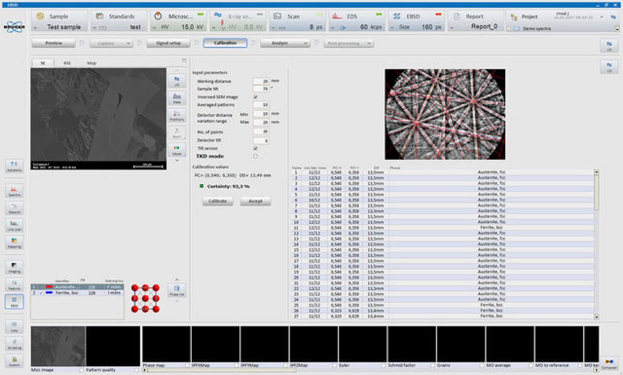
EBSD indexing and crystallographic analysis with Bruker ESPRIT.
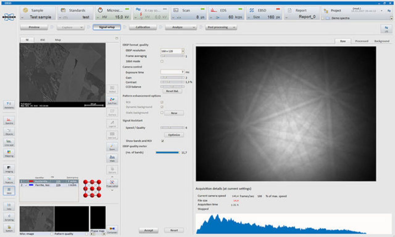
Kikuchi pattern used for crystallographic orientation analysis.
SEM Imaging and Elemental Analysis
Beyond crystallographic analysis, the NANOS EBSD retains the imaging capabilities of the NANOS platform. A secondary electron detector provides detailed surface information, while a four-quadrant backscattered electron detector adds compositional contrast and topographical information.
In the EDS configuration, a fully integrated silicon drift detector extends the system with elemental analysis. Point analysis, line scans and elemental mapping can be used alongside SEM imaging, allowing structural, compositional and crystallographic information to be investigated on the same platform.
Sample Handling, Vacuum and Sample Requirements
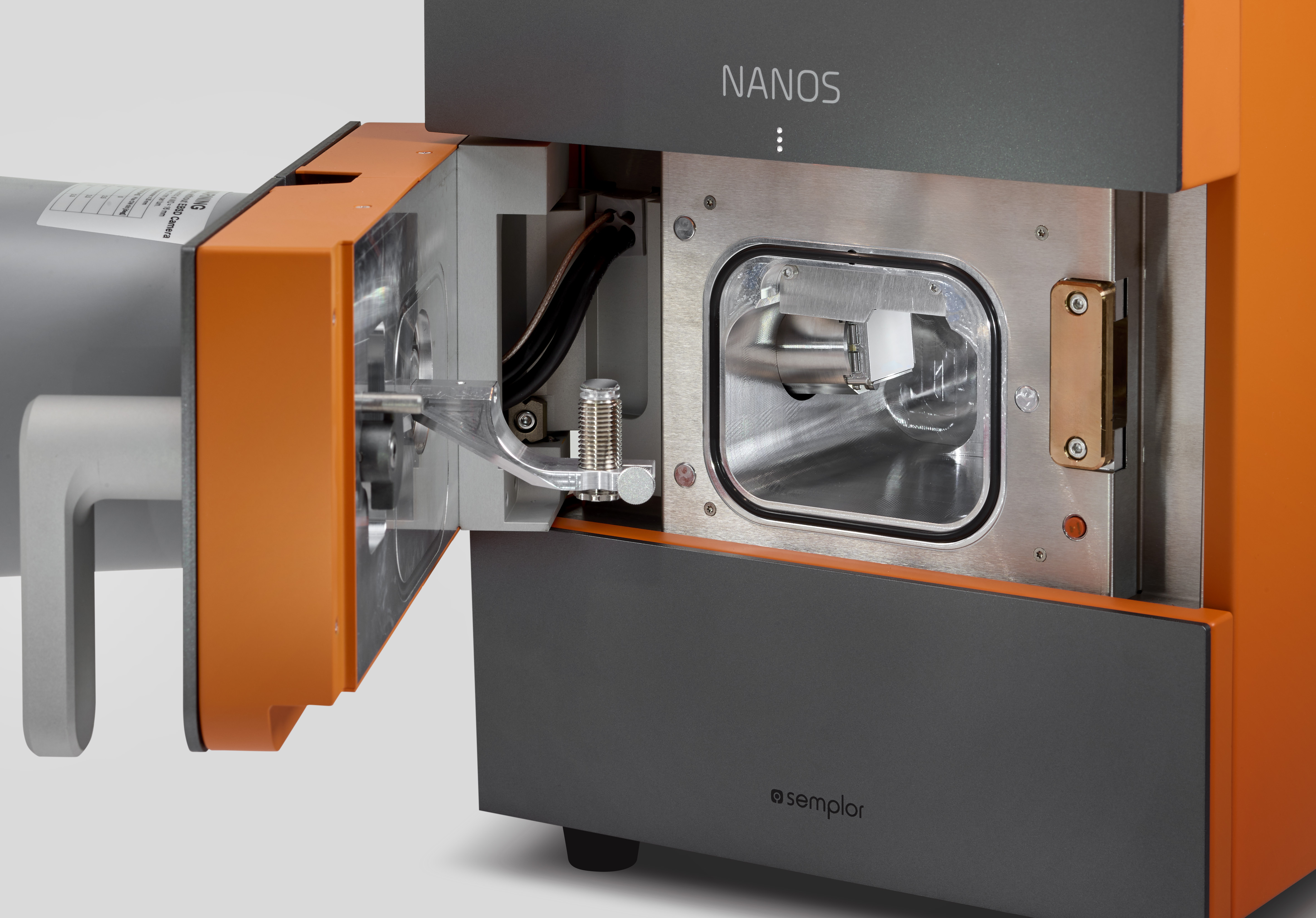
The NANOS EBSD uses the compact sample-handling concept of the NANOS platform, with motorized XY movement and high- and low-vacuum operation. The eucentric stage supports the transition between SEM imaging and the 70° EBSD measurement position while keeping the selected area of interest centered.
Because EBSD requires a defined detector and sample geometry, the usable sample dimensions depend on the installed EBSD configuration and the required tilt position. Sample size, holder geometry and the available tilt range therefore need to be considered together when configuring the system for a specific application.
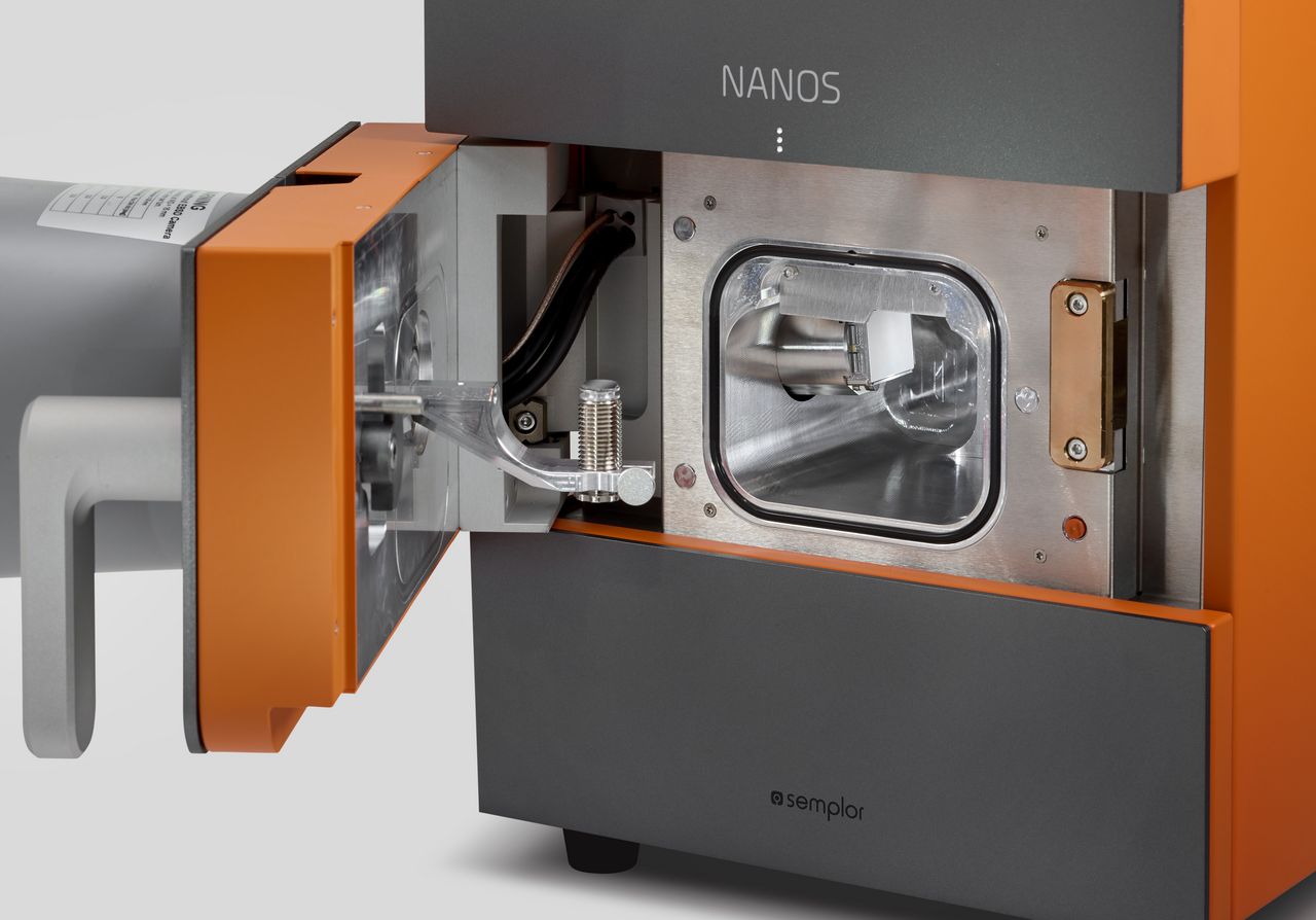
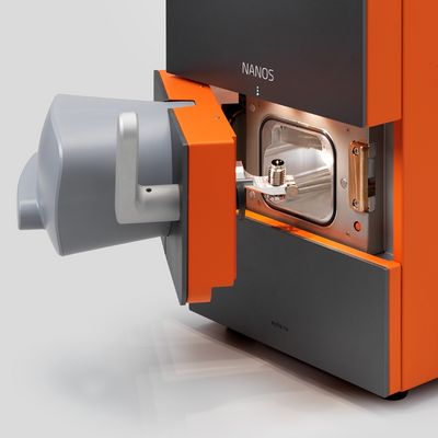
Open sample chamber of the NANOS EBSD.
Specifications
Electron Optics and Imaging
| SEM Resolution | < 8 nm |
|---|---|
| Magnification | 100x to 200,000x |
| Image Resolution | up to 4096 x 4096 pixels |
| Accelerating Voltages | 1, 2, 5, 7, 10, 15 and 20 kV |
| Electron Source | optimized thermionic tungsten source |
| Secondary Electron Detector | SED |
| Backscattered Electron Detector | four-quadrant BSE detector |
Electron Backscatter Diffraction (EBSD)
| Detector | Bruker e-Flash XS |
|---|---|
| Detector Technology | CMOS imaging chip |
| Native Image Resolution | 720 x 540 pixels |
| Binning Modes | 2x2, 3x3, 4x4, 5x5, 6x6 |
| Pattern Acquisition Rate | up to 520 frames per second |
| Optics | optical system with field lens |
| Phosphor Screen | user-replaceable |
| Connection | USB 3.0 for data and power |
| Scan Generator | QUANTAX Scan system |
| Analysis Software | Bruker ESPRIT |
EDS
| Detector | thermoelectrically cooled silicon drift detector |
|---|---|
| Active Area | 30 mm² |
| Energy Resolution | < 132 eV at Mn Kα |
| Maximum Input Count Rate | 300,000 cps |
| Analysis | point analysis, line analysis and elemental mapping |
Sample Stage and Vacuum
| XY Travel | motorized, 12.5 x 12.5 mm |
|---|---|
| Sample Tilt | manual, eucentric; imaging position to 70° EBSD position |
| Maximum Sample Diameter | 12.5 mm |
| Maximum Sample Height | 17.5 mm |
| Vacuum Modes | high vacuum and low vacuum |
| Low Vacuum | 40 Pa |
System Data
| Dimensions | 280 (W) x 470 (D) x 550 (H) mm |
|---|---|
| Weight | 62 kg |
| Vacuum Pumps | Pfeiffer turbomolecular pump and oil-free membrane pre-vacuum pump |
| Workstation | pre-configured All-in-One PC with 27" monitor |
| Temperature | 15-25 °C |
| Relative Humidity | 20-80% |
| Power Consumption | typically 110 W; max. 140 W |
Applications
The NANOS EBSD is designed for crystallographic characterization of crystalline materials. Typical applications include:
- Crystal orientation mapping: spatially resolved analysis of local crystal orientations across the sample
- Phase identification and phase distribution: identification and differentiation of crystalline phases
- Grain structure analysis: reconstruction of grains and evaluation of grain size, shape and orientation
- Grain boundary and misorientation analysis: characterization of grain boundaries and local orientation differences
- Texture analysis: evaluation of crystallographic orientation distributions and preferred orientations
- Combined structural and elemental characterization: complementary use of EBSD and EDS information within the same analytical platform
Downloads
Contact


| +49 6157 80710-557 | |
| +49 6157 807109557 | |
| Write e-mail |

Navigation
Categories
Contact
Quantum Design GmbH
Breitwieserweg 9
64319 Pfungstadt
Germany
| Phone: | +49 6157 80710-0 |
| E-mail: | germanyqd-europe.com |
Support